Samsung patents 3D chip design with interlocking guard rings
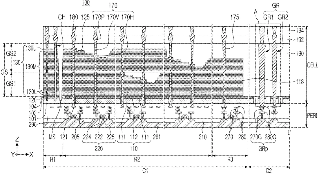
Samsung describes a semiconductor structure for 3D memory chips that uses a guard ring to protect the active storage area. This ring is made of two parts with interlocking bumps that fit together like puzzle pieces to seal the edge of the chip.
In the filing’s own words
In example embodiments, provided is a semiconductor device including: a guard ring structure surrounding an active region and penetrating through a cell region insulating layer and an upper insulating layer, and the guard ring structure includes: a first structure including a first body portion penetrating through the cell region insulating layer and extending in a second direction, substantially perpendicular to the first direction, and first protrusion portions protruding from an upper surface of the first body portion and spaced apart from one another; and a second structure including second body portion penetrating through the upper insulating layer so as to overlap the first structure in the first direction on the first structure, and second protrusion portions protruding from a lower surface of the second body portion and spaced apart from one another, and the first protrusion portions and the second protrusion portions are disposed alternately in the second direction.
What exactly they claim (claim 1)
1. A semiconductor device, comprising: a substrate including an active region and an edge region surrounding the active region; a stack structure including a plurality of gate electrodes stacked and spaced apart from one another in a first direction, substantially perpendicular to an upper surface of the substrate, in the active region; a channel structure penetrating through the stack structure in the first direction and including a channel layer; a cell region insulating layer disposed in the edge region; an upper insulating layer disposed on the cell region insulating layer; and a guard ring structure surrounding the active region and penetrating through the cell region insulating layer and the upper insulating layer, in the edge region, wherein the guard ring structure includes: a first structure including a first body portion penetrating through the cell region insulating layer from the substrate and extending in a second direction, substantially perpendicular to the first direction, and first protrusion portions protruding from an upper surface of the first body portion and spaced apart from one another; and a second structure including second body portion penetrating through the upper insulating layer so as to overlap the first structure in the first direction on the first structure, and second protrusion portions protruding from a lower surface of the second body portion and spaced apart from one another, wherein the first protrusion portions and the second protrusion portions are disposed alternately in the second direction.
Facts
- Company
- Samsung (Samsung Electronics Co., Ltd.)
- Official title
- SEMICONDUCTOR DEVICES INCLUDING GUARD RING STRUCTURE AND DATA STORAGE SYSTEMS INCLUDING THE SAME
- Publication number
- US20260313905A1
- Application number
- 19369835
- Filed
- Oct 27, 2025
- Published
- Oct 8, 2026
- Inventors
- 3
- Claims
- 20
Classified under
H10B 43/50 Electricity & electronicsH10B 41/27 Electricity & electronicsH10B 41/35 Electricity & electronicsH10B 41/50 Electricity & electronicsH10B 43/27 Electricity & electronicsH10B 43/35 Electricity & electronicsMore from Samsung in Chips & hardware
- Samsung patents chip that combines camera and screen Oct 13, 2026
- Samsung patents faster chip testing using machine learning Sep 1, 2026
- Samsung patents radar method to pinpoint target direction more accurately Sep 1, 2026
- Samsung patents memory chip that searches data by content, not address Sep 1, 2026
- Samsung patents chip design that skips empty data to speed up AI Sep 1, 2026
Summaries are simplified from the filing’s own abstract and first claim. A patent filing is not a product announcement.
Patent data and drawings: U.S. Patent and Trademark Office (USPTO). Nebula is not affiliated with or endorsed by the USPTO.