Samsung patents a two-step masking method for making semiconductor chips
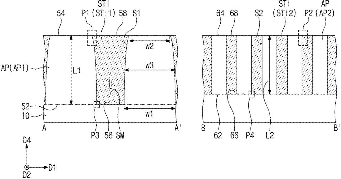
Samsung describes a specific way to build parts of a computer chip using two layers of protective material called masks. The process involves creating patterns on these layers and carefully removing parts of them to expose different sections of the chip base for further processing.
In the filing’s own words
A method of fabricating a semiconductor device includes sequentially forming a lower mask layer and an upper mask layer on a substrate having a first region and a second region therein, forming a first mask pattern and a second mask pattern, which are respectively placed on the first region and the second region, on the upper mask layer, removing a portion of the upper mask layer, which is exposed by the second mask pattern, from the second region, then removing the first mask pattern from the first region, and forming an upper mask pattern by etching a remaining portion of the upper mask layer on the first region and on the second region, using the second mask pattern as an etch mask, the upper mask pattern covering the lower mask layer on the first region and exposes a portion of the lower mask layer on the second region.
What exactly they claim (claim 1)
1 - 20. (canceled)
Facts
- Company
- Samsung (Samsung Electronics Co., Ltd.)
- Official title
- SEMICONDUCTOR DEVICE AND METHOD OF FABRICATING THE SAME
- Publication number
- US20260313885A1
- Application number
- 19711840
- Filed
- Jun 17, 2026
- Published
- Oct 8, 2026
- Inventors
- 5
- Claims
- 21
Classified under
H10B 12/50 Electricity & electronicsH10B 12/01 Electricity & electronicsH10W 10/0145 Electricity & electronicsH10W 10/17 Electricity & electronicsH10B 12/315 Electricity & electronicsMore from Samsung in Chips & hardware
- Samsung patents chip that combines camera and screen Oct 13, 2026
- Samsung patents faster chip testing using machine learning Sep 1, 2026
- Samsung patents radar method to pinpoint target direction more accurately Sep 1, 2026
- Samsung patents memory chip that searches data by content, not address Sep 1, 2026
- Samsung patents chip design that skips empty data to speed up AI Sep 1, 2026
Summaries are simplified from the filing’s own abstract and first claim. A patent filing is not a product announcement.
Patent data and drawings: U.S. Patent and Trademark Office (USPTO). Nebula is not affiliated with or endorsed by the USPTO.