Samsung patents vapor chamber cooling for phone chips
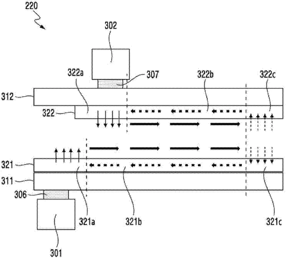
Samsung describes an electronic device that uses a vapor chamber to cool two separate heat sources, a display driver and a processor. The chamber contains two distinct wick structures with specific paths that move heat away from each component without overlapping.
In the filing’s own words
An electronic device includes: a housing; a first heat source and a second heat source in the housing; a vapor chamber between the first heat source and the second heat source. The vapor chamber includes: a first plate to be closer to the first heat source than the second heat source, a second plate to be closer to the second heat source than the first heat source, a first wick in the internal space and in contact with at least a part of an inner side of the first plate. The first wick includes a plurality of first holes. A second wick is disposed in the internal space and in contact with at least a part of an inner side of the second plate. The second wick includes a plurality of second holes.
What exactly they claim (claim 1)
1. An electronic device comprising: a housing; a display panel defining at least a part of a front side of the housing; a display driver integrated circuit (DDI) connected to the display panel and closer to a top side of the housing than a bottom side of the housing; a processor in the housing and comprising processing circuitry; and a vapor chamber between the DDI and the processor, wherein the vapor chamber comprises: a first heat conductivity member disposed to dissipate heat generated by the DDI and including a first plate and a first wick in contact with the first plate, and a second heat conductivity member disposed to dissipate heat generated by the processor and including a second plate and a second wick in contact with the second plate, wherein the first wick is disposed in an internal space disposed between the first plate and the second plate and includes: a first evaporation portion overlapping at least a part of the DDI and receiving heat generated by the DDI, a first condensation portion spaced apart from the DDI and receiving heat from the DDI, and a first path portion connecting the first evaporation portion to the first condensation portion, wherein the second wick is disposed in the internal space and includes: a second evaporation portion overlapping at least a part of the processor and receiving heat generated by the processor, a second condensation portion spaced apart from the processor, and a second path portion connecting the second evaporation portion to the second condensation portion, and wherein the first path portion of the first wick and the second path portion of the second wick do not overlap each other.
Facts
- Company
- Samsung (SAMSUNG ELECTRONICS CO., LTD.)
- Official title
- ELECTRONIC DEVICE INCLUDING VAPOR CHAMBER
- Publication number
- US20260313843A1
- Application number
- 19444970
- Filed
- Jan 9, 2026
- Published
- Oct 8, 2026
- Inventors
- 7
- Claims
- 20
Classified under
H05K 7/20336 Electricity & electronicsH05K 5/02 Electricity & electronicsH05K 7/20309 Electricity & electronicsH05K 7/20318 Electricity & electronicsMore from Samsung in Chips & hardware
- Samsung patents chip that combines camera and screen Oct 13, 2026
- Samsung patents faster chip testing using machine learning Sep 1, 2026
- Samsung patents radar method to pinpoint target direction more accurately Sep 1, 2026
- Samsung patents memory chip that searches data by content, not address Sep 1, 2026
- Samsung patents chip design that skips empty data to speed up AI Sep 1, 2026
Summaries are simplified from the filing’s own abstract and first claim. A patent filing is not a product announcement.
Patent data and drawings: U.S. Patent and Trademark Office (USPTO). Nebula is not affiliated with or endorsed by the USPTO.