Samsung patents storage method that adjusts erase voltage based on cell status
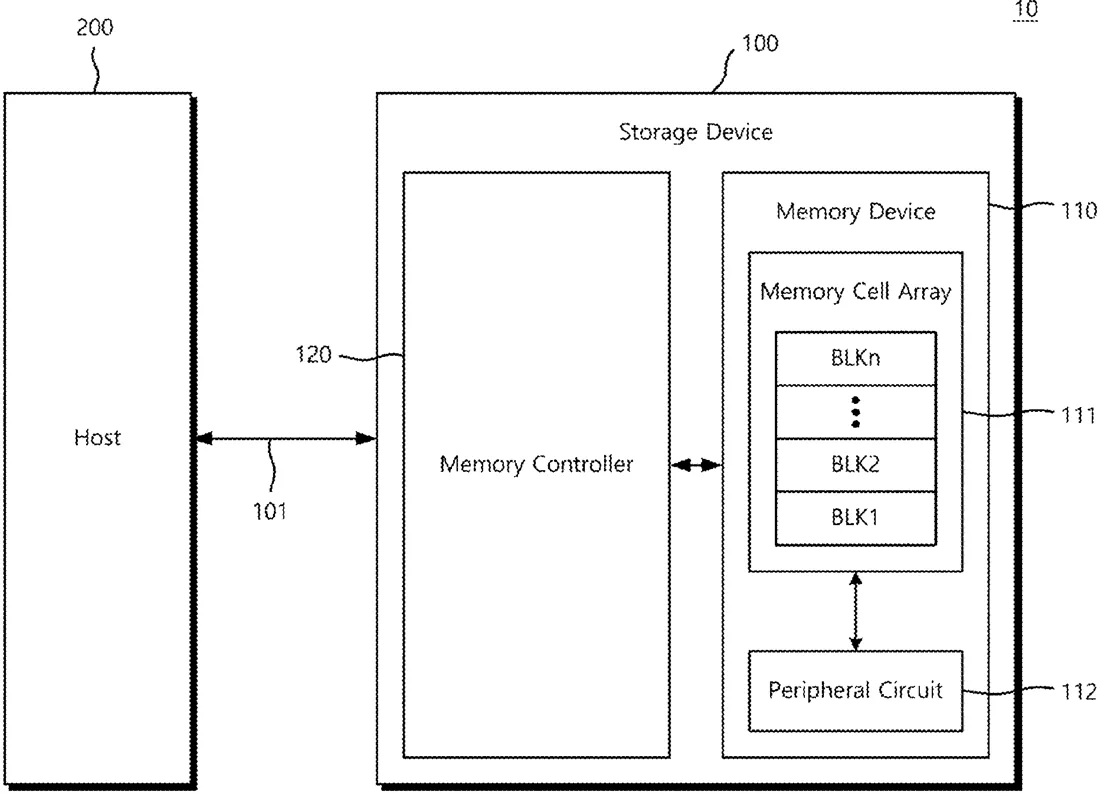
This filing describes a method for operating memory storage where the device checks how many cells failed to erase properly after an initial command. If too many cells remain 'off,' the system increases the voltage used for the next erase attempt to ensure the data is cleared.
In the filing’s own words
A method of operating a storage device includes applying a first erase voltage to a first memory block, among a plurality of memory blocks, in response to a first erase command for the first memory block, determining a number of off-cells, each having a threshold voltage greater than or equal to a reference voltage, among memory cells included in the first memory block, obtaining a second erase voltage by adding a unit erase voltage to the first erase voltage in response to the number of the off-cells exceeding a reference number, and applying the second erase voltage to the first memory block in response to a second erase command for the first memory block.
What exactly they claim (claim 1)
1. A method of operating a storage device, the method comprising: applying a first erase voltage to a first memory block, among a plurality of memory blocks, in response to a first erase command for the first memory block; determining a number of off-cells, each having a threshold voltage greater than or equal to a reference voltage, among memory cells included in the first memory block; obtaining a second erase voltage by adding a unit erase voltage to the first erase voltage in response to the number of the off-cells exceeding a reference number; and applying the second erase voltage to the first memory block in response to a second erase command for the first memory block.
Facts
- Company
- Samsung (Samsung Electronics Co., Ltd.)
- Official title
- STORAGE DEVICE UPDATING OPERATION VOLTAGES BASED ON A NUMBER OF OFF CELLS AND METHOD OF OPERATING THE SAME
- Publication number
- US20260311770A1
- Application number
- 19458161
- Filed
- Jan 23, 2026
- Published
- Oct 8, 2026
- Inventors
- 3
- Claims
- 20
Classified under
G11C 16/14 Physics & computingG11C 16/0483 Physics & computingG11C 16/08 Physics & computingG11C 16/10 Physics & computingG11C 16/26 Physics & computingMore from Samsung in Chips & hardware
- Samsung patents chip that combines camera and screen Oct 13, 2026
- Samsung patents faster chip testing using machine learning Sep 1, 2026
- Samsung patents radar method to pinpoint target direction more accurately Sep 1, 2026
- Samsung patents memory chip that searches data by content, not address Sep 1, 2026
- Samsung patents chip design that skips empty data to speed up AI Sep 1, 2026
Summaries are simplified from the filing’s own abstract and first claim. A patent filing is not a product announcement.
Patent data and drawings: U.S. Patent and Trademark Office (USPTO). Nebula is not affiliated with or endorsed by the USPTO.