Samsung patents memory method using electron tunneling to improve data storage
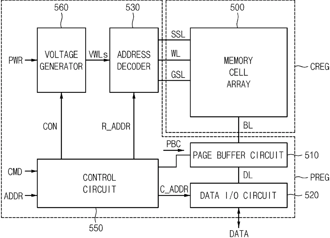
Samsung describes a method for operating nonvolatile memory, a type of storage that keeps data without power. The process involves erasing data, then using specific electrical voltages to push electrons into a small gap between storage areas before writing new data.
In the filing’s own words
A method of operating a nonvolatile memory device includes sequentially performing an erase operation, a back-tunneling electron-injection operation, and a program operation. The erase operation is performed to release electrons in charge storage regions of a plurality of memory cells of the nonvolatile memory device. The back-tunneling electron-injection operation is performed to inject electrons into a spacer region between a charge storage region corresponding to a target wordline and a charge storage region corresponding to a neighboring wordline adjacent to the target wordline by applying a back-tunneling voltage to the target wordline and a boosting voltage higher than the back-tunneling voltage to the neighboring wordline. The program operation is performed to inject electrons into the charge storage region corresponding to the target wordline.
What exactly they claim (claim 1)
1. A method of operating a nonvolatile memory device, comprising: performing an erase operation to release a first set of electrons at a plurality of charge storage regions of a plurality of memory cells of the nonvolatile memory device; after performing the erase operation, performing, based on applying a back-tunneling voltage to a target wordline and a boosting voltage greater than the back-tunneling voltage to a neighboring wordline adjacent to the target wordline, back-tunneling electron-injection operation to inject a second set of electrons of the electrons into a spacer region between (i) a first charge storage region of the plurality of charge storage regions that corresponds to the target wordline and (ii) a second charge storage region of the plurality of charge storage regions that corresponds to the neighboring wordline; and after performing the back-tunneling electron-injection operation, performing a program operation to inject a third set of electrons of the electrons into the first charge storage region.
Facts
- Company
- Samsung (Samsung Electronics Co., Ltd.)
- Official title
- NONVOLATILE MEMORY DEVICE AND METHOD OF OPERATING THE SAME
- Publication number
- US20260311769A1
- Application number
- 19451809
- Filed
- Jan 16, 2026
- Published
- Oct 8, 2026
- Inventors
- 7
- Claims
- 20
Classified under
G11C 16/14 Physics & computingG11C 16/0483 Physics & computingG11C 16/08 Physics & computingMore from Samsung in Chips & hardware
- Samsung patents chip that combines camera and screen Oct 13, 2026
- Samsung patents faster chip testing using machine learning Sep 1, 2026
- Samsung patents radar method to pinpoint target direction more accurately Sep 1, 2026
- Samsung patents memory chip that searches data by content, not address Sep 1, 2026
- Samsung patents chip design that skips empty data to speed up AI Sep 1, 2026
Summaries are simplified from the filing’s own abstract and first claim. A patent filing is not a product announcement.
Patent data and drawings: U.S. Patent and Trademark Office (USPTO). Nebula is not affiliated with or endorsed by the USPTO.