Samsung patents stacked memory chips with split control lines
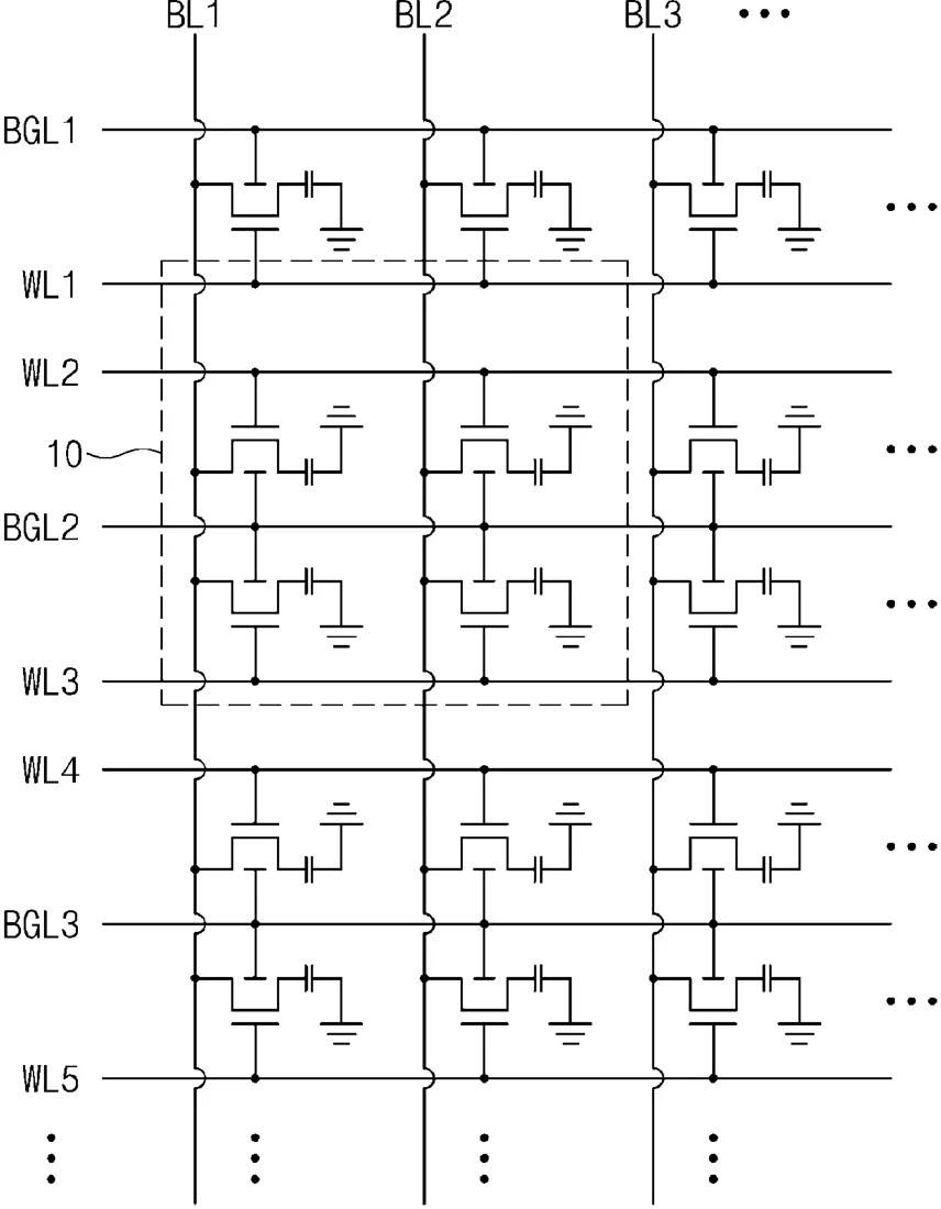
Samsung describes a memory design where two chip layers are stacked vertically. The top layer holds the data storage lines, which are split into two groups separated by a shared control line, while the bottom layer contains the drivers that activate those lines.
In the filing’s own words
A semiconductor memory device includes a first semiconductor die and a second semiconductor die. The first semiconductor die and the second semiconductor die are stacked in a vertical direction. The first semiconductor die includes a first wordline group, a second wordline group, and a first backgateline. The first wordline group includes wordlines that are adjacent to each other and multiples of two. The first backgateline is disposed between the first wordline group and the second wordline group. The second semiconductor die includes a first sub-wordline driver group and a second sub-wordline driver group. The first sub-wordline driver group drives the first wordline group. The second sub-wordline driver group drives the second wordline group.
What exactly they claim (claim 1)
1. A semiconductor memory device comprising: a first semiconductor die; and a second semiconductor die, the first semiconductor die and the second semiconductor die being stacked in a vertical direction, wherein the first semiconductor die includes: a first wordline group including a first plurality of wordlines that are adjacent to each other; a second wordline group including a second plurality of wordlines that are adjacent to each other; and a first backgateline between the first wordline group and the second wordline group, wherein the second semiconductor die includes: a first sub-wordline driver group configured to drive the first wordline group; and a second sub-wordline driver group configured to drive the second wordline group.
Facts
- Company
- Samsung (Samsung Electronics Co., Ltd.)
- Official title
- SEMICONDUCTOR MEMORY DEVICES WITH WORDLINE GROUPS
- Publication number
- US20260311741A1
- Application number
- 19431024
- Filed
- Dec 23, 2025
- Published
- Oct 8, 2026
- Inventors
- 4
- Claims
- 20
Classified under
G11C 11/4085 Physics & computingG11C 11/4091 Physics & computingMore from Samsung in Chips & hardware
- Samsung patents chip that combines camera and screen Oct 13, 2026
- Samsung patents faster chip testing using machine learning Sep 1, 2026
- Samsung patents radar method to pinpoint target direction more accurately Sep 1, 2026
- Samsung patents memory chip that searches data by content, not address Sep 1, 2026
- Samsung patents chip design that skips empty data to speed up AI Sep 1, 2026
Summaries are simplified from the filing’s own abstract and first claim. A patent filing is not a product announcement.
Patent data and drawings: U.S. Patent and Trademark Office (USPTO). Nebula is not affiliated with or endorsed by the USPTO.