Samsung patents AI method to optimize chip design for better performance
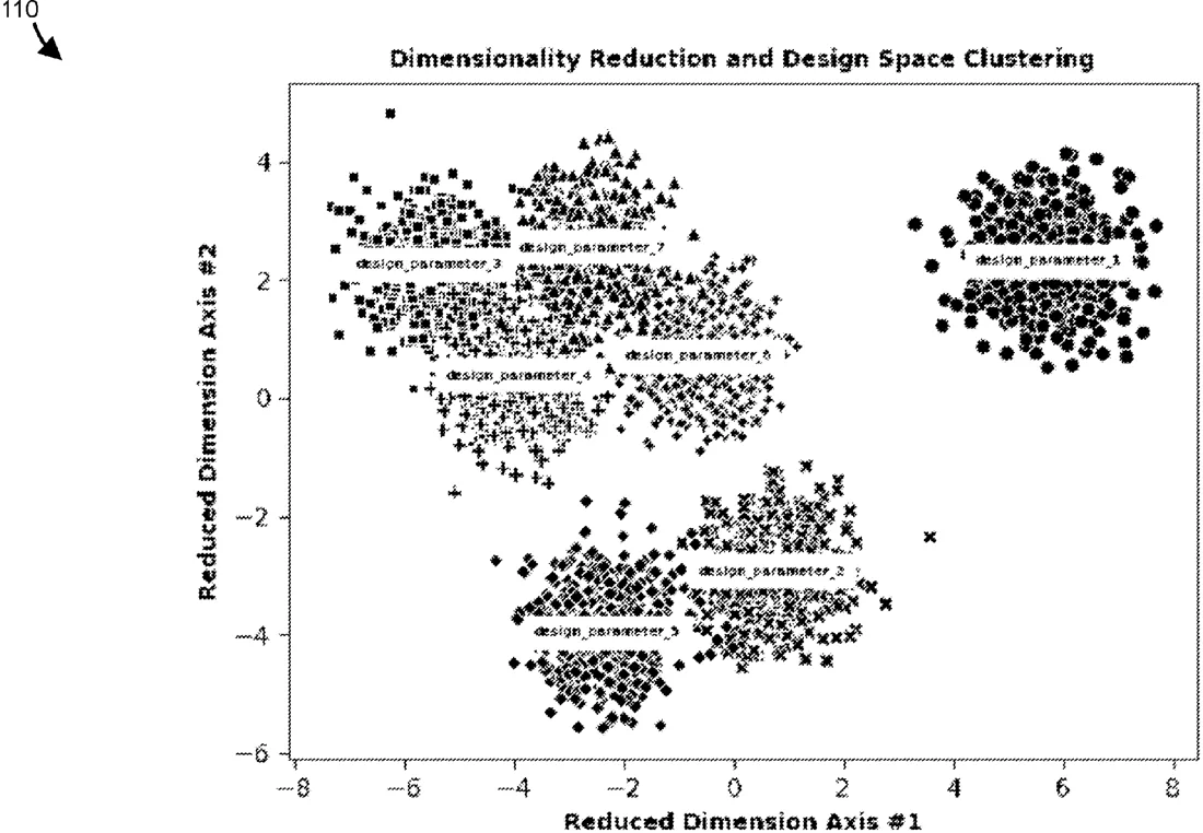
Samsung has filed a patent application for a method that uses artificial intelligence to improve the power, performance, and area efficiency of semiconductor chips. The system analyzes chip design features, reduces their complexity using machine learning techniques, and selects optimal design elements from a library to enhance the final chip layout.
In the filing’s own words
A system and method are disclosed for improving power/performance/area (PPA) of a semiconductor chip design, the method comprising: refining a set of PPA features of the semiconductor chip design; reducing a dimensionality of the set of PPA features by applying a variational autoencoder (VAE) or clustering; selecting, for a respective design block within the semiconductor chip design, a respective highly ranked design element from a library of technology design elements based on the reduced dimensionality; and applying the respective highly ranked design element to the respective design block to improve PPA of a semiconductor chip having the semiconductor chip design.
What exactly they claim (claim 1)
1. A method of improving power/performance/area (PPA) of a semiconductor chip design, comprising: refining a set of PPA features of the semiconductor chip design; reducing a dimensionality of the set of PPA features by applying a variational autoencoder (VAE) or clustering; selecting, for a respective design block within the semiconductor chip design, a respective highly ranked design element from a library of technology design elements, based on the reduced dimensionality; applying the respective highly ranked design element to the respective design block within the semiconductor chip design to obtain an updated semiconductor chip design with improved PPA; and outputting the updated semiconductor chip design for a semiconductor chip with improved PPA.
Facts
- Company
- Samsung (Samsung Electronics Co., Ltd.)
- Official title
- METHODS AND APPARATUS FOR IMPROVING CHIP DESIGN WITH DESIGN TECHNOLOGY CO-OPTIMIZATION USING ARTIFICIAL INTELLIGENCE AND MACHINE LEARNING
- Publication number
- US20260310870A1
- Application number
- 19347375
- Filed
- Oct 1, 2025
- Published
- Oct 8, 2026
- Inventors
- 4
- Claims
- 20
Classified under
G06F 30/337 Physics & computingG06F 30/27 Physics & computingG06F 2119/06 Physics & computingMore from Samsung in Chips & hardware
- Samsung patents chip that combines camera and screen Oct 13, 2026
- Samsung patents faster chip testing using machine learning Sep 1, 2026
- Samsung patents radar method to pinpoint target direction more accurately Sep 1, 2026
- Samsung patents memory chip that searches data by content, not address Sep 1, 2026
- Samsung patents chip design that skips empty data to speed up AI Sep 1, 2026
Summaries are simplified from the filing’s own abstract and first claim. A patent filing is not a product announcement.
Patent data and drawings: U.S. Patent and Trademark Office (USPTO). Nebula is not affiliated with or endorsed by the USPTO.