Samsung patents chip that adjusts speed based on memory traffic
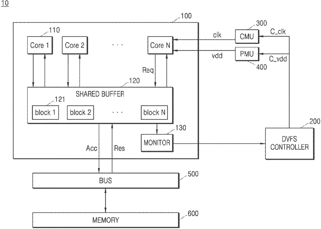
This filing describes a processor design that watches how busy its internal data storage is to decide how fast each core should run. Instead of guessing, it measures how long data takes to arrive from outside memory and adjusts the voltage and frequency accordingly to match the actual workload.
In the filing’s own words
Provided are an integrated circuit capable of classifying a workload of a core based on monitored data and performing a dynamic voltage and frequency scaling (DVFS) operation based on the classified workload, and an operating method of the integrated circuit. The integrated circuit includes at least one core, a shared buffer which receives a request from the at least one core, access an external memory according to the request, and receive a response from the external memory, a monitor which monitors the shared buffer to obtain a buffer capacity of the shared buffer and a response waiting time, and a DVFS controller configured to classify a workload of the at least one core.
What exactly they claim (claim 1)
1. A device comprising at least one integrated circuit, the integrated circuit comprising: a plurality of cores configured to process an instruction according to a voltage-frequency level; a shared buffer, comprising a plurality of blocks, configured to receive a request including data designating a certain block among the plurality of blocks from a first core of the plurality of cores, access an external memory according to the request, and receive a response from the external memory, wherein each of the plurality of blocks is configured to access a corresponding designated region among a plurality of regions of the external memory; a monitor configured to monitor the shared buffer to obtain a buffer capacity of the shared buffer, the buffer capacity corresponding to a number of respective ones of the plurality of blocks each using a threshold capacity being greater than or equal to a threshold number among the plurality of blocks, a response waiting time for the response received from the external memory, and an identifier of the first core; and a dynamic voltage and frequency scaling (DVFS) controller configured to receive, from the monitor, the buffer capacity, the response waiting time and the identifier, and to identify the first core according to the identifier and classify a workload of the first core based on the buffer capacity and the response waiting time, and determine a scaling factor for the voltage-frequency level of the first core based on the classified workload.
Facts
- Company
- Samsung (Samsung Electronics Co., Ltd.)
- Official title
- INTEGRATED CIRCUIT CAPABLE OF PERFORMING DYNAMIC VOLTAGE AND FREQUENCY SCALING OPERATION BASED ON WORKLOAD AND OPERATING METHOD THEREOF
- Publication number
- US20260310272A1
- Application number
- 19709712
- Filed
- Jun 16, 2026
- Published
- Oct 8, 2026
- Inventors
- 1
- Claims
- 19
Classified under
G06F 1/26 Physics & computingMore from Samsung in Chips & hardware
- Samsung patents chip that combines camera and screen Oct 13, 2026
- Samsung patents faster chip testing using machine learning Sep 1, 2026
- Samsung patents radar method to pinpoint target direction more accurately Sep 1, 2026
- Samsung patents memory chip that searches data by content, not address Sep 1, 2026
- Samsung patents chip design that skips empty data to speed up AI Sep 1, 2026
Summaries are simplified from the filing’s own abstract and first claim. A patent filing is not a product announcement.
Patent data and drawings: U.S. Patent and Trademark Office (USPTO). Nebula is not affiliated with or endorsed by the USPTO.