Samsung patents math trick to fix tiny errors in chip masks
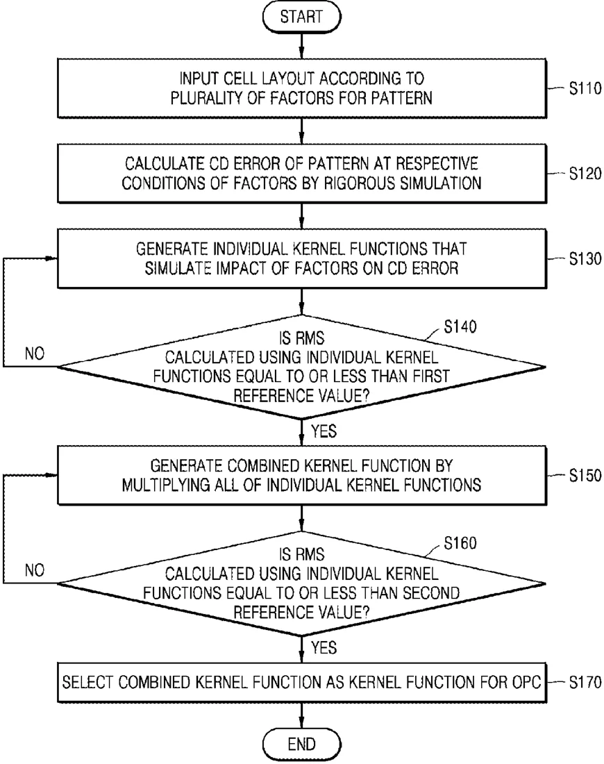
Samsung describes a method to improve how computer chips are made by correcting tiny size errors in the design. The system calculates how different factors affect the final size of the chip patterns and combines these calculations into a single correction tool. This tool is then used to adjust the mask, which acts as a stencil for creating the chip.
In the filing’s own words
A kernel function is generated for accurately predicting a critical dimension (CD) error in a unit block edge (UBE) region as well as in a center region. An optical proximity correction (OPC) method uses the kernel function. A mask manufacturing method includes the OPC method. The method of generating a kernel function includes inputting data of a cell layout according to a plurality of factors for a pattern, calculating a CD error of a pattern under conditions of the factors, generating individual kernel functions that simulate the impact of the factors on the CD error, and generating a combined kernel function by multiplying all of the individual kernel functions.
What exactly they claim (claim 1)
1. A method of generating a kernel function, the method comprising: providing data of a cell layout according to a plurality of factors for a pattern; calculating, by one or more processors, a respective critical dimension (CD) error of the pattern for each factor of the plurality of factors under varying conditions of remaining factors of the plurality of factors; generating, by the one or more processors, and for each CD error, individual kernel functions that simulate an impact of each factor of the plurality of factors on the CD error; generating, by the one or more processors, a combined kernel function by multiplying the individual kernel functions; performing an optical proximity correction on the cell layout data using the combined kernel function; and exposing a mask substrate based on the optical proximity corrected cell layout data.
Facts
- Company
- Samsung (Samsung Electronics Co., Ltd.)
- Official title
- KERNEL FUNCTION GENERATION METHOD, OPTICAL PROXIMITY CORRECTION METHOD USING THE KERNEL FUNCTION, AND MASK MANUFACTURING METHOD INCLUDING THE OPTICAL PROXIMITY CORRECTION METHOD
- Publication number
- US20260310064A1
- Application number
- 19410497
- Filed
- Dec 5, 2025
- Published
- Oct 8, 2026
- Inventors
- 3
- Claims
- 20
Classified under
G03F 1/36 Physics & computingG03F 1/70 Physics & computingG06F 30/398 Physics & computingG06F 2119/18 Physics & computingMore from Samsung in Chips & hardware
- Samsung patents chip that combines camera and screen Oct 13, 2026
- Samsung patents faster chip testing using machine learning Sep 1, 2026
- Samsung patents radar method to pinpoint target direction more accurately Sep 1, 2026
- Samsung patents memory chip that searches data by content, not address Sep 1, 2026
- Samsung patents chip design that skips empty data to speed up AI Sep 1, 2026
Summaries are simplified from the filing’s own abstract and first claim. A patent filing is not a product announcement.
Patent data and drawings: U.S. Patent and Trademark Office (USPTO). Nebula is not affiliated with or endorsed by the USPTO.