Samsung patents 3D mask model for chip manufacturing
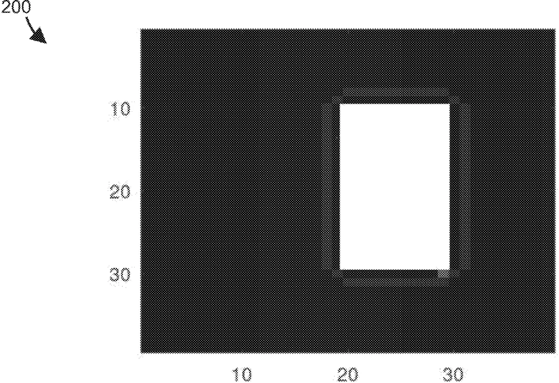
Samsung has filed a patent for a method to improve optical proximity correction in semiconductor manufacturing. The system uses the Huygens-Fresnel principle to calculate how light spreads when passing through a mask, creating a 3D model of the light pattern. This helps predict the exact shape of the circuit patterns etched onto silicon wafers.
In the filing’s own words
A system and method are provided for an image-based mask model in optical proximity correction. A method includes obtaining a mask shape, determining a point spread function (PSF) of a two-dimensional spatial frequency based on a line spread function (LSF) of a one-dimensional spatial frequency having a magnitude substantially equal to a magnitude of the two-dimensional spatial frequency, applying the PSF to the mask shape to obtain a three-dimensional (3D) mask effect, generating an aerial image based on the at least one 3D mask effect, and generating a resist contour based on the aerial image.
What exactly they claim (claim 1)
1. An optical proximity correction (OPC) method for photolithography in semiconductor technology, the method comprising: obtaining at least one mask shape; applying an image-based mask model for the photolithography to the at least one mask shape, wherein applying the image-based mask model comprises: determining a point spread function (PSF) of a two-dimensional spatial frequency based on a line spread function (LSF) of a one-dimensional spatial frequency having a magnitude substantially equal to a magnitude of the two-dimensional spatial frequency; and applying the PSF to the at least one mask shape to obtain a three-dimensional (3D) mask effect; generating, based on the 3D mask effect, an aerial image indicating a projected light pattern resulting from the photolithography; and generating, based on the aerial image, a resist contour indicating a resist pattern on a semiconductor wafer.
Facts
- Company
- Samsung (Samsung Electronics Co., Ltd.)
- Official title
- SYSTEM AND METHOD FOR 3D MASK MODEL BASED ON HUYGENS-FRESNEL PRINCIPLE
- Publication number
- US20260310063A1
- Application number
- 19303697
- Filed
- Aug 19, 2025
- Published
- Oct 8, 2026
- Inventors
- 8
- Claims
- 20
Classified under
G03F 1/36 Physics & computingG03F 7/70441 Physics & computingMore from Samsung in Chips & hardware
- Samsung patents chip that combines camera and screen Oct 13, 2026
- Samsung patents faster chip testing using machine learning Sep 1, 2026
- Samsung patents radar method to pinpoint target direction more accurately Sep 1, 2026
- Samsung patents memory chip that searches data by content, not address Sep 1, 2026
- Samsung patents chip design that skips empty data to speed up AI Sep 1, 2026
Summaries are simplified from the filing’s own abstract and first claim. A patent filing is not a product announcement.
Patent data and drawings: U.S. Patent and Trademark Office (USPTO). Nebula is not affiliated with or endorsed by the USPTO.