Samsung patents method to predict radiation damage in chips
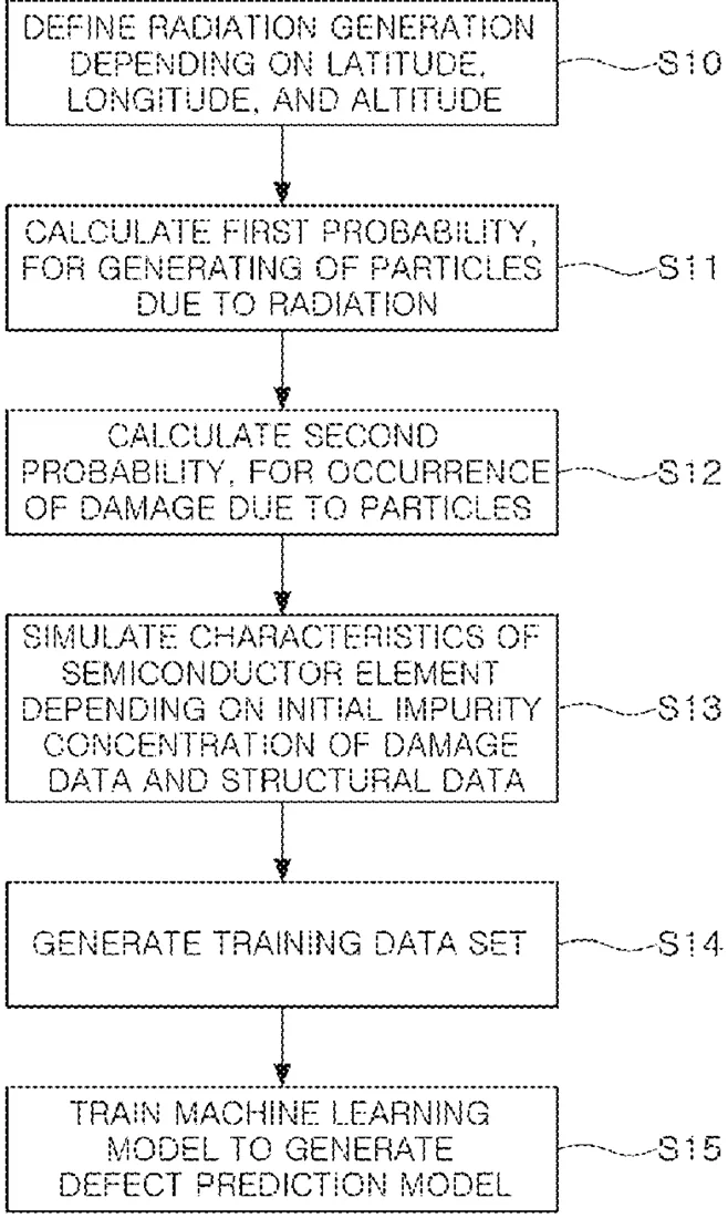
Samsung describes a way to check if a computer chip has been damaged by radiation, such as from space or medical equipment. The method uses a computer model to compare the chip's electrical resistance against a healthy baseline to estimate the likelihood of failure.
In the filing’s own words
A method for predicting a defect in a semiconductor device using a defect prediction model, the method includes obtaining reference data on resistance of a semiconductor element of the semiconductor device under conditions in which damage caused by radiation has not occurred, inputting input data of conditions in which damage caused by radiation has occurred to the defect prediction model to obtain prediction data on the resistance of the semiconductor element, predicting an element defect probability of the semiconductor element caused by damage from radiation using the reference data and the prediction data, and calculating a device defect probability of the semiconductor device comprising the semiconductor element using the element defect probability.
What exactly they claim (claim 1)
1. A method for predicting a defect in a semiconductor device using a defect prediction model, the method comprising: obtaining reference data on resistance of a semiconductor element of the semiconductor device under conditions in which damage caused by radiation has not occurred; inputting input data of conditions in which damage caused by radiation has occurred to the defect prediction model to obtain prediction data on the resistance of the semiconductor element; predicting an element defect probability of the semiconductor element caused by damage from radiation using the reference data and the prediction data; and calculating a device defect probability of the semiconductor device comprising the semiconductor element using the element defect probability.
Facts
- Company
- Samsung (Samsung Electronics Co., Ltd.)
- Official title
- METHOD FOR PREDICTING DEFECT IN SEMICONDUCTOR DEVICE
- Publication number
- US20260309768A1
- Application number
- 19715915
- Filed
- Jun 22, 2026
- Published
- Oct 8, 2026
- Inventors
- 9
- Claims
- 20
Classified under
G01R 31/2848 Physics & computingG01T 1/24 Physics & computingG06F 30/20 Physics & computingG06N 20/00 Physics & computingG06T 7/0008 Physics & computingH10P 72/0616 Electricity & electronicsMore from Samsung in Chips & hardware
- Samsung patents chip that combines camera and screen Oct 13, 2026
- Samsung patents faster chip testing using machine learning Sep 1, 2026
- Samsung patents radar method to pinpoint target direction more accurately Sep 1, 2026
- Samsung patents memory chip that searches data by content, not address Sep 1, 2026
- Samsung patents chip design that skips empty data to speed up AI Sep 1, 2026
Summaries are simplified from the filing’s own abstract and first claim. A patent filing is not a product announcement.
Patent data and drawings: U.S. Patent and Trademark Office (USPTO). Nebula is not affiliated with or endorsed by the USPTO.