Samsung patents dark field system for spotting tiny defects on chips
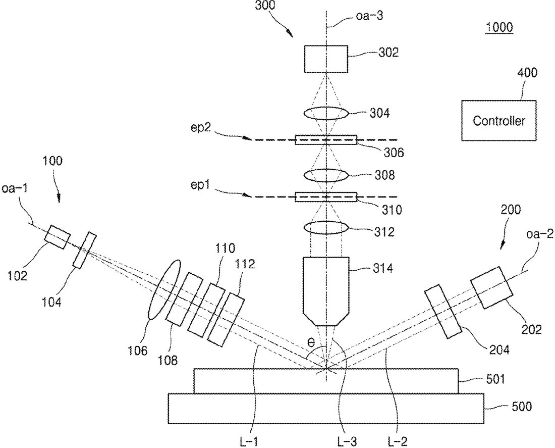
Samsung describes a machine that shines light at a steep angle onto a surface to find tiny flaws. It uses specific lenses and filters to separate the scattered light from defects from the main beam, allowing for precise detection.
In the filing’s own words
A dark field defect inspection system includes a stage on which an inspection substrate is arranged, an illumination optical system radiating incident light to a top surface of the inspection substrate and arranged along a first oblique optical axis rotated in a first rotation direction from a normal line to the top surface of the inspection substrate, a calibration optical system receiving calibration light and arranged along a second oblique optical axis rotated in a second rotation direction opposite to the first rotation direction from the normal line, and an inspection optical system receiving inspection light and arranged along a vertical optical axis extending upward from the inspection substrate. The inspection optical system includes an inspection analyzer arranged after the objective lens along the vertical optical axis and an aperture arranged along the vertical optical axis and arranged in an exit pupil plane of the objective lens.
What exactly they claim (claim 1)
1. A dark field defect inspection system comprising: a stage on which an inspection substrate is arranged; an illumination optical system configured to radiate incident light to a top surface of the inspection substrate and arranged along a first oblique optical axis rotated in a first rotation direction from a normal line to the top surface of the inspection substrate by an oblique angle; a calibration optical system configured to receive calibration light and arranged along a second oblique optical axis rotated in a second rotation direction from the normal line by the oblique angle, the second rotation direction being opposite to the first rotation direction; and an inspection optical system configured to receive inspection light and arranged along a vertical optical axis extending upward from the inspection substrate, wherein the illumination optical system includes: a light source configured to output the incident light; a delivery optical system configured to shape the incident light output from the light source into a preset shape, the delivery optical system including at least one lens; a first phase retardation plate and a second phase retardation plate each configured to delay a phase of the incident light; and a linear polarizer arranged between the first phase retardation plate and the second phase retardation plate, the inspection optical system includes: an inspection detector configured to receive the inspection light; an objective lens facing an inspection region of the inspection substrate; a tube lens arranged before the inspection detector along the vertical optical axis; an inspection analyzer arranged after the objective lens along the vertical optical axis; and an aperture arranged along the vertical optical axis and arranged in an exit pupil plane of the objective lens, the delivery optical system of the illumination optical system includes a cylindrical lens arranged between the first phase retardation plate and the light source along the first oblique optical axis, the exit pupil plane of the objective lens includes a virtual plane on which the inspection light exiting the objective lens converges, the oblique angle is about 50 degrees to about 75 degrees, and the calibration light and the inspection light include scattered light from the inspection substrate.
Facts
- Company
- Samsung (Samsung Electronics Co., Ltd.)
- Official title
- DARK FIELD DEFECT INSPECTION SYSTEM AND INSPECTION METHOD THEREOF
- Publication number
- US20260309637A1
- Application number
- 19391199
- Filed
- Nov 17, 2025
- Published
- Oct 8, 2026
- Inventors
- 8
- Claims
- 20
Classified under
G01N 21/8806 Physics & computingG01N 21/211 Physics & computingG01N 21/956 Physics & computingG01N 2021/8822 Physics & computingG01N 2021/8848 Physics & computingG01N 2201/0683 Physics & computingMore from Samsung in Chips & hardware
- Samsung patents chip that combines camera and screen Oct 13, 2026
- Samsung patents faster chip testing using machine learning Sep 1, 2026
- Samsung patents radar method to pinpoint target direction more accurately Sep 1, 2026
- Samsung patents memory chip that searches data by content, not address Sep 1, 2026
- Samsung patents chip design that skips empty data to speed up AI Sep 1, 2026
Summaries are simplified from the filing’s own abstract and first claim. A patent filing is not a product announcement.
Patent data and drawings: U.S. Patent and Trademark Office (USPTO). Nebula is not affiliated with or endorsed by the USPTO.