Samsung patents chip package design with layered metal connections
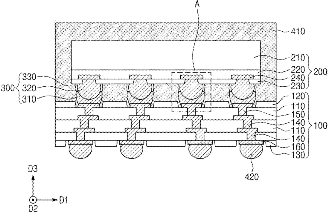
Samsung has filed a patent for a semiconductor package that links two separate structures using a specific connection method. The design uses a lower metal conductor and an upper metal conductor, with an insulating material surrounding the top part to keep the electrical signals separated.
In the filing’s own words
A semiconductor package includes a first structure that includes an upper connection pattern; a second structure that includes a lower connection pattern; and a connection structure that connects the upper connection pattern of the first structure to the lower connection pattern of the second structure, wherein the connection structure includes a lower conductor connected to the upper connection pattern of the first structure; an upper conductor connected to the lower conductor and the lower connection pattern of the second structure; and a dielectric pattern that at least partially surrounds the upper conductor, and the dielectric pattern includes a first surface in contact with the upper conductor; and a second surface in contact with the lower conductor.
What exactly they claim (claim 1)
1. A semiconductor package, comprising: a connection structure including a lower conductor, an upper conductor connected to the lower conductor, and a dielectric pattern that at least partially surrounds the upper conductor; a first structure including an upper connection pattern connected to the lower conductor; and a second structure including a lower connection pattern connected to the upper conductor, wherein the upper connection pattern of the first structure includes a sidewall forming a portion of an outer surface of the first structure, and wherein the lower conductor covers at least a portion of the sidewall.
Facts
- Company
- Samsung (Samsung Electronics Co., Ltd.)
- Official title
- SEMICONDUCTOR PACKAGE AND METHOD OF FABRICATING THE SAME
- Publication number
- US20260305278A1
- Application number
- 19703293
- Filed
- Jun 10, 2026
- Published
- Oct 1, 2026
- Inventors
- 3
- Claims
- 20
Classified under
H10W 20/01 Electricity & electronicsH10W 20/4403 Electricity & electronicsH10W 74/016 Electricity & electronicsH10W 90/00 Electricity & electronicsH10W 90/701 Electricity & electronicsH10W 90/751 Electricity & electronicsMore from Samsung in Chips & hardware
- Samsung patents chip that combines camera and screen Oct 13, 2026
- Samsung patents faster chip testing using machine learning Sep 1, 2026
- Samsung patents radar method to pinpoint target direction more accurately Sep 1, 2026
- Samsung patents memory chip that searches data by content, not address Sep 1, 2026
- Samsung patents chip design that skips empty data to speed up AI Sep 1, 2026
Summaries are simplified from the filing’s own abstract and first claim. A patent filing is not a product announcement.
Patent data and drawings: U.S. Patent and Trademark Office (USPTO). Nebula is not affiliated with or endorsed by the USPTO.