Microsoft patents metal box design for quantum signal amplifiers
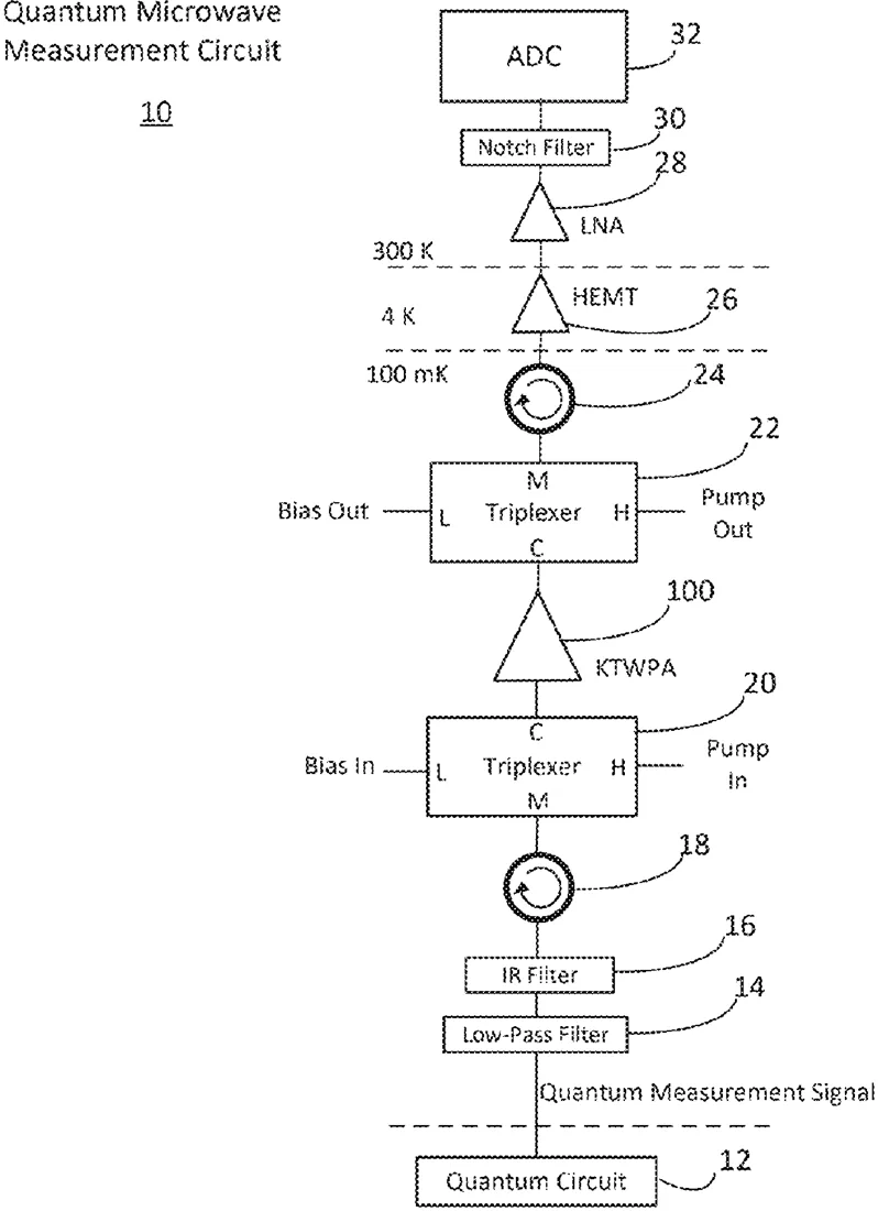
Microsoft describes a specific metal enclosure for a quantum amplifier that uses a superconducting line to boost weak signals. The design includes a silicon chip, wire bonds, and a copper lid that connects to the main housing to manage heat and electricity. This packaging helps place the amplifier inside a quantum measurement circuit.
In the filing’s own words
A kinetic inductance travelling-wave parametric amplifier (KTWPA) device is provided that includes a metallic enclosure having a base including an inside top surface, sides, and an enclosure lid, a substrate coupled to the inside top surface of the base, the substrate including a plurality of conductive pads, a silicon die including a superconducting transmission line, the silicon die coupled to the substrate, a plurality of conductive spacers coupled to the silicon die, wire bonds attached between the conductive pads and the silicon die, and a copper lid coupled to the top end of the plurality of conductive spacer, where the copper lid is electrically and thermally coupled to the enclosure lid. The KTWPA device may be applied in a quantum microwave measurement circuit to amplify a quantum measurement signal from a quantum circuit.
What exactly they claim (claim 1)
1. A kinetic inductance travelling-wave parametric amplifier (KTWPA) device, comprising: a metallic enclosure having a base including an inside top surface, sides, and an enclosure lid, the metallic enclosure forming a cavity; a substrate bonded to the inside top surface of the base, the substrate including a plurality of conductive pads; a silicon die including a superconducting transmission line, the silicon die coupled to the substrate; a plurality of conductive spacers, each having a top end and a bottom end, the bottom end of the plurality of conductive spacers coupled to the silicon die; a plurality of wire bonds coupled between the plurality of conductive pads and the silicon die; and a copper lid coupled to the top end of the plurality of conductive spacers, wherein the copper lid is electrically and thermally coupled to the enclosure lid.
Facts
- Company
- Microsoft (Microsoft Technology Licensing, LLC)
- Official title
- PACKAGING OF KINETIC INDUCTANCE TRAVELLING-WAVE PARAMETRIC AMPLIFIER (KTWPA) DEVICE
- Publication number
- US20260303046A1
- Application number
- 19096141
- Filed
- Mar 31, 2025
- Published
- Oct 1, 2026
- Inventors
- 3
- Claims
- 20
Classified under
H03F 7/02 Electricity & electronicsMore from Microsoft in Chips & hardware
- Microsoft patents chips with liquid cooling built inside Oct 1, 2026
- Microsoft patents chip design that guesses code steps ahead Sep 8, 2026
- Microsoft patents 3D glass storage using laser light patterns Sep 8, 2026
- Microsoft patents hand-held radar reflectors for tracking movement Sep 8, 2026
- Microsoft patents video boost that reuses old frames to save power Sep 15, 2026
Summaries are simplified from the filing’s own abstract and first claim. A patent filing is not a product announcement.
Patent data and drawings: U.S. Patent and Trademark Office (USPTO). Nebula is not affiliated with or endorsed by the USPTO.