Samsung patents memory chip that fixes bad rows using stored addresses
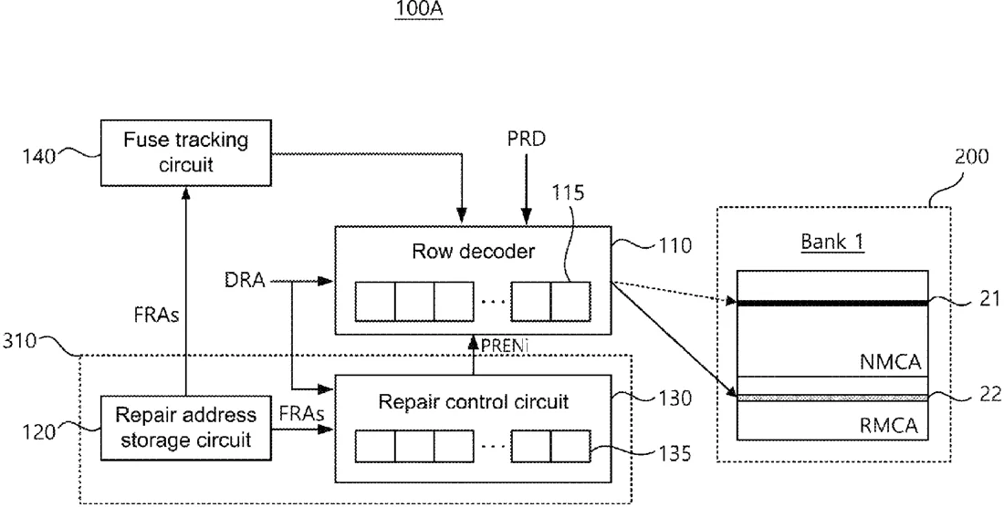
This filing describes a high bandwidth memory (HBM) chip that stores the locations of faulty rows in a fuse array. When the chip turns on, a control circuit reads these addresses to identify which specific row decoder blocks need adjustment, allowing the system to bypass or repair the defective areas.
In the filing’s own words
A memory device includes a row decoder including a plurality of row decoder blocks arranged in series, wherein the plurality of row decoder blocks are distinguished based on row addresses which the plurality of row decoder blocks take charge of; a repair address storage circuit including a fuse array in which a first plurality of faulty row addresses are stored; a repair control circuit including a plurality of repair control blocks arranged in series to correspond to the plurality of row decoder blocks; and a fuse tracking circuit configured to determine locations of row decoder blocks corresponding to a second plurality of faulty row addresses among the first plurality of faulty row addresses received from the repair address storage circuit and to control an operation of the row decoder based on the locations.
What exactly they claim (claim 1)
1. A high bandwidth memory (HBM) device comprising: a plurality of dies including a first die and a second die vertically stacked on the first die, wherein the first die comprises: a repair address storage circuit comprising a fuse array in which a faulty row address is stored; a repair control circuit configured to receive the faulty row address from the repair address storage circuit based on the HBM device being turned on; a row decoder including a row decoder block corresponding to the faulty row address; and a control circuit configured to determine a location of the row decoder block and to generate a control signal for controlling an operation of the row decoder based on the determined location.
Facts
- Company
- Samsung (SAMSUNG ELECTRONICS CO., LTD.)
- Official title
- MEMORY DEVICE AND OPERATING METHOD THEREOF
- Publication number
- US20260300109A1
- Application number
- 19699776
- Filed
- Jun 5, 2026
- Published
- Oct 1, 2026
- Inventors
- 2
- Claims
- 3
Classified under
G06F 11/1666 Physics & computingG06F 11/073 Physics & computingG06F 11/0793 Physics & computingG06F 11/16 Physics & computingG06F 11/1612 Physics & computingG06F 11/2094 Physics & computingMore from Samsung in Chips & hardware
- Samsung patents chip that combines camera and screen Oct 13, 2026
- Samsung patents faster chip testing using machine learning Sep 1, 2026
- Samsung patents radar method to pinpoint target direction more accurately Sep 1, 2026
- Samsung patents memory chip that searches data by content, not address Sep 1, 2026
- Samsung patents chip design that skips empty data to speed up AI Sep 1, 2026
Summaries are simplified from the filing’s own abstract and first claim. A patent filing is not a product announcement.
Patent data and drawings: U.S. Patent and Trademark Office (USPTO). Nebula is not affiliated with or endorsed by the USPTO.