Samsung patents chip package with built-in light connector
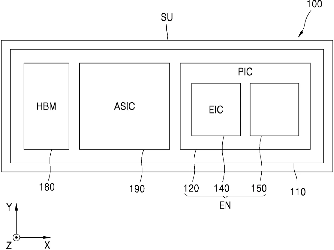
Samsung describes a processor package that combines a standard chip, memory, and a light-based communication module on a single base. The design includes a specific groove structure to help align tiny glass fibers with the light circuit for better data transfer.
In the filing’s own words
A processor package includes an interposer, a memory on the interposer, a processor on the interposer, and an optical engine on the interposer, where the optical engine includes a photonic integrated circuit (PIC) chip including circuit elements configured for photoelectric conversion, and a coupling structure on the PIC chip and configured to provide a light input/output path, and the coupling structure includes, on an upper portion thereof, at least one groove structure configured for alignment with a fiber array unit (FAU).
What exactly they claim (claim 1)
1. A processor package comprising: an interposer; a memory on the interposer; a processor on the interposer; and an optical engine on the interposer, wherein the optical engine comprises: a photonic integrated circuit (PIC) chip comprising circuit elements configured for photoelectric conversion; and a coupling structure on the PIC chip and configured to provide a light input/output path, and wherein the coupling structure comprises, on an upper portion thereof, at least one groove structure configured for alignment with a fiber array unit (FAU).
Facts
- Company
- Samsung (SAMSUNG ELECTRONICS CO., LTD.)
- Official title
- PROCESSOR PACKAGE INTEGRATED WITH OPTICAL ENGINE, ELECTRONIC DEVICE INCLUDING THE PROCESSOR PACKAGE, AND METHOD OF MANUFACTURING THE PROCESSOR PACKAGE
- Publication number
- US20260299227A1
- Application number
- 19566336
- Filed
- Mar 13, 2026
- Published
- Oct 1, 2026
- Inventors
- 2
- Claims
- 20
Classified under
G02B 6/4249 Physics & computingG02B 6/4204 Physics & computingG02B 6/4243 Physics & computingG02B 6/4261 Physics & computingG02B 6/428 Physics & computingH10B 80/00 Electricity & electronicsMore from Samsung in Chips & hardware
- Samsung patents chip that combines camera and screen Oct 13, 2026
- Samsung patents faster chip testing using machine learning Sep 1, 2026
- Samsung patents radar method to pinpoint target direction more accurately Sep 1, 2026
- Samsung patents memory chip that searches data by content, not address Sep 1, 2026
- Samsung patents chip design that skips empty data to speed up AI Sep 1, 2026
Summaries are simplified from the filing’s own abstract and first claim. A patent filing is not a product announcement.
Patent data and drawings: U.S. Patent and Trademark Office (USPTO). Nebula is not affiliated with or endorsed by the USPTO.