Samsung patents optical film with reflective pads for better light control
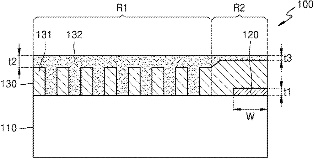
Samsung has filed a patent for an optical device that uses a multilayered film structure to manage how light passes through. The design includes a nanostructure layer with specific patterns and a reflective pad placed underneath inactive areas to bounce light back, using materials with different light-bending properties to improve performance.
In the filing’s own words
An optical apparatus includes a lower optical layer; a nanostructure layer disposed on the lower optical layer and having an active region and a non-active region; and a reflective pad disposed between the lower optical layer and the nanostructure layer to face the non-active region of the nanostructure layer, wherein the nanostructure layer includes a first dielectric patterned in the active region and unpatterned in the non-active region and a second dielectric filled between patterns of the first dielectric, and the first dielectric includes a first material and the second dielectric includes a second material different from the first material and having a different refractive index from a refractive index of the first material.
What exactly they claim (claim 1)
1. An optical apparatus comprising: a lower optical layer; a nanostructure layer disposed on the lower optical layer, the nanostructure layer comprising an active region and a non-active region; and a reflective pad disposed between the lower optical layer and the nanostructure layer to face the non-active region of the nanostructure layer, wherein the nanostructure layer comprises a first dielectric patterned in the active region and unpatterned in the non-active region and a second dielectric filled between patterns of the first dielectric, wherein the first dielectric comprises a first material and the second dielectric comprises a second material different from the first material and having a different refractive index from a refractive index of the first material, wherein an edge of the reflective pad proximate to the active region is disposed away from a boundary between the active region and the non-active region to form an offset away from the boundary, wherein a size of the reflective pad is smaller than a size of the non-active region.
Facts
- Company
- Samsung (SAMSUNG ELECTRONICS CO., LTD.)
- Official title
- OPTICAL APPARATUS INCLUDING MULTILAYERED OPTICAL FILM STRUCTURE AND METHOD AND APPARATUS FOR PLANARIZING THE MULTILAYERED OPTICAL FILM STRUCTURE
- Publication number
- US20260299179A1
- Application number
- 19695350
- Filed
- Jun 2, 2026
- Published
- Oct 1, 2026
- Inventors
- 4
- Claims
- 20
Classified under
G02B 5/285 Physics & computingMore from Samsung in Chips & hardware
- Samsung patents chip that combines camera and screen Oct 13, 2026
- Samsung patents faster chip testing using machine learning Sep 1, 2026
- Samsung patents radar method to pinpoint target direction more accurately Sep 1, 2026
- Samsung patents memory chip that searches data by content, not address Sep 1, 2026
- Samsung patents chip design that skips empty data to speed up AI Sep 1, 2026
Summaries are simplified from the filing’s own abstract and first claim. A patent filing is not a product announcement.
Patent data and drawings: U.S. Patent and Trademark Office (USPTO). Nebula is not affiliated with or endorsed by the USPTO.