Samsung patents laser system to check material quality
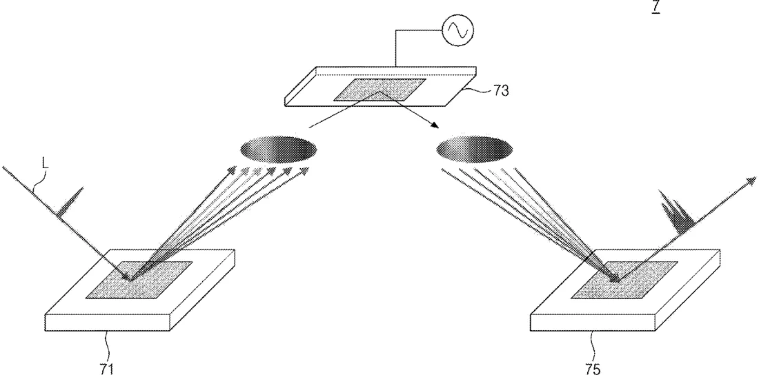
Samsung describes a device that splits a laser beam into two parts to inspect the surface of a material. One part of the beam is adjusted using a modulator and compared against the other to detect flaws or changes in the substrate.
In the filing’s own words
A substrate inspection apparatus includes a laser light source configured to emit a laser beam, an optical splitter configured to split the laser beam into a first laser beam and a second laser beam, a delay stage configured to change a relative time delay of the second laser beam and optically connected to the optical splitter, a first modulator optically connected to the optical splitter and configured to change the first laser beam, and a feedback system configured to sense the second laser beam reflected from a substrate and configured to apply electrical feedback to the first modulator.
What exactly they claim (claim 1)
1. A method of inspecting a substrate, the method comprising: disposing the substrate in a substrate inspection apparatus; and inspecting the substrate, wherein the substrate inspection apparatus comprises: a laser light source configured to emit a laser beam; an optical splitter configured to split the laser beam into a first laser beam and a second laser beam; a delay stage configured to receive the second laser beam from the optical splitter and configured to change a frequency of the second laser beam relative to the first laser beam; and a modulator optically connected to the optical splitter or the delay stage and configured to change a wavefront of the laser beam or an intensity of the laser beam for each frequency, wherein the modulator comprises an optical modulator configured to change the laser beam, wherein the optical modulator comprises a spatial light modulator or a piezoelectric transducer, and wherein inspecting the substrate comprises: splitting the laser beam emitted from the laser light source into the first laser beam and the second laser beam by the optical splitter; changing the first laser beam or the second laser beam by the modulator; and irradiating the first laser beam and the second laser beam onto the substrate.
Facts
- Company
- Samsung (SAMSUNG ELECTRONICS CO., LTD.)
- Official title
- SUBSTRATE INSPECTION APPARATUS AND METHOD OF INSPECTING A SUBSTRATE USING THE SAME
- Publication number
- US20260299005A1
- Application number
- 19706125
- Filed
- Jun 12, 2026
- Published
- Oct 1, 2026
- Inventors
- 7
- Claims
- 20
Classified under
G01R 31/2656 Physics & computingMore from Samsung in Chips & hardware
- Samsung patents chip that combines camera and screen Oct 13, 2026
- Samsung patents faster chip testing using machine learning Sep 1, 2026
- Samsung patents radar method to pinpoint target direction more accurately Sep 1, 2026
- Samsung patents memory chip that searches data by content, not address Sep 1, 2026
- Samsung patents chip design that skips empty data to speed up AI Sep 1, 2026
Summaries are simplified from the filing’s own abstract and first claim. A patent filing is not a product announcement.
Patent data and drawings: U.S. Patent and Trademark Office (USPTO). Nebula is not affiliated with or endorsed by the USPTO.