Samsung patents non-destructive way to check chip layers during manufacturing
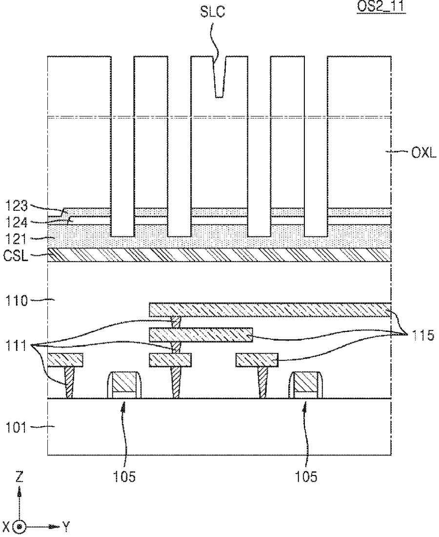
Samsung describes a method for inspecting semiconductor memory devices without damaging them. It uses sound or light-based techniques to measure specific layers at different stages of production, then calculates the final structure's properties from this data.
In the filing’s own words
A method of manufacturing a semiconductor device may include: forming a plurality of process observation sites by sequentially performing a series of unit processes on a substrate; forming a target structure including a structure of interest by performing an additional process on the plurality of process observation sites; inspecting at least some of the plurality of process observation sites and inspecting the target structure, each of the inspecting being performed by any one from among an optoacoustic inspection and an ultrasonic inspection, thereby obtaining measurement data regarding the at least some of the plurality of process observation sites and the target structure; and obtaining extracted data, which is data regarding the structure of interest of the target structure, based on calculations on the measurement data regarding the at least some of the plurality of process observation sites and the target structure.
What exactly they claim (claim 1)
1. A method of manufacturing a semiconductor device, the method comprising: forming a plurality of process observation sites by sequentially performing a series of unit processes on a substrate; forming a target structure including a structure of interest by performing an additional process on the plurality of process observation sites; inspecting at least some of the plurality of process observation sites and inspecting the target structure, each of the inspecting being performed by any one from among an optoacoustic inspection and an ultrasonic inspection, thereby obtaining measurement data regarding the at least some of the plurality of process observation sites and the target structure; and obtaining extracted data, which is data regarding the structure of interest of the target structure, based on calculations on the measurement data regarding the at least some of the plurality of process observation sites and the target structure, wherein the at least some of the plurality of process observation sites are intermediate results of forming the target structure, and wherein the inspecting of the at least some of the plurality of process observation sites is performed prior to formation of the target structure.
Facts
- Company
- Samsung (SAMSUNG ELECTRONICS CO., LTD.)
- Official title
- NON-DESTRUCTIVE INSPECTION METHOD INCLUDING INSPECTING MULTIPLE OBSERVATION SITES AND METHOD OF MANUFACTURING SEMICONDUCTOR MEMORY DEVICE USING THE SAME
- Publication number
- US20260298804A1
- Application number
- 19702459
- Filed
- Jun 9, 2026
- Published
- Oct 1, 2026
- Inventors
- 4
- Claims
- 20
Classified under
G01N 21/1702 Physics & computingG01N 21/9501 Physics & computingH10B 43/27 Electricity & electronicsH10P 74/203 Electricity & electronicsH10P 74/27 Electricity & electronicsG01N 2021/1706 Physics & computingMore from Samsung in Chips & hardware
- Samsung patents chip that combines camera and screen Oct 13, 2026
- Samsung patents faster chip testing using machine learning Sep 1, 2026
- Samsung patents radar method to pinpoint target direction more accurately Sep 1, 2026
- Samsung patents memory chip that searches data by content, not address Sep 1, 2026
- Samsung patents chip design that skips empty data to speed up AI Sep 1, 2026
Summaries are simplified from the filing’s own abstract and first claim. A patent filing is not a product announcement.
Patent data and drawings: U.S. Patent and Trademark Office (USPTO). Nebula is not affiliated with or endorsed by the USPTO.