Samsung patents thin film method with longer plasma step
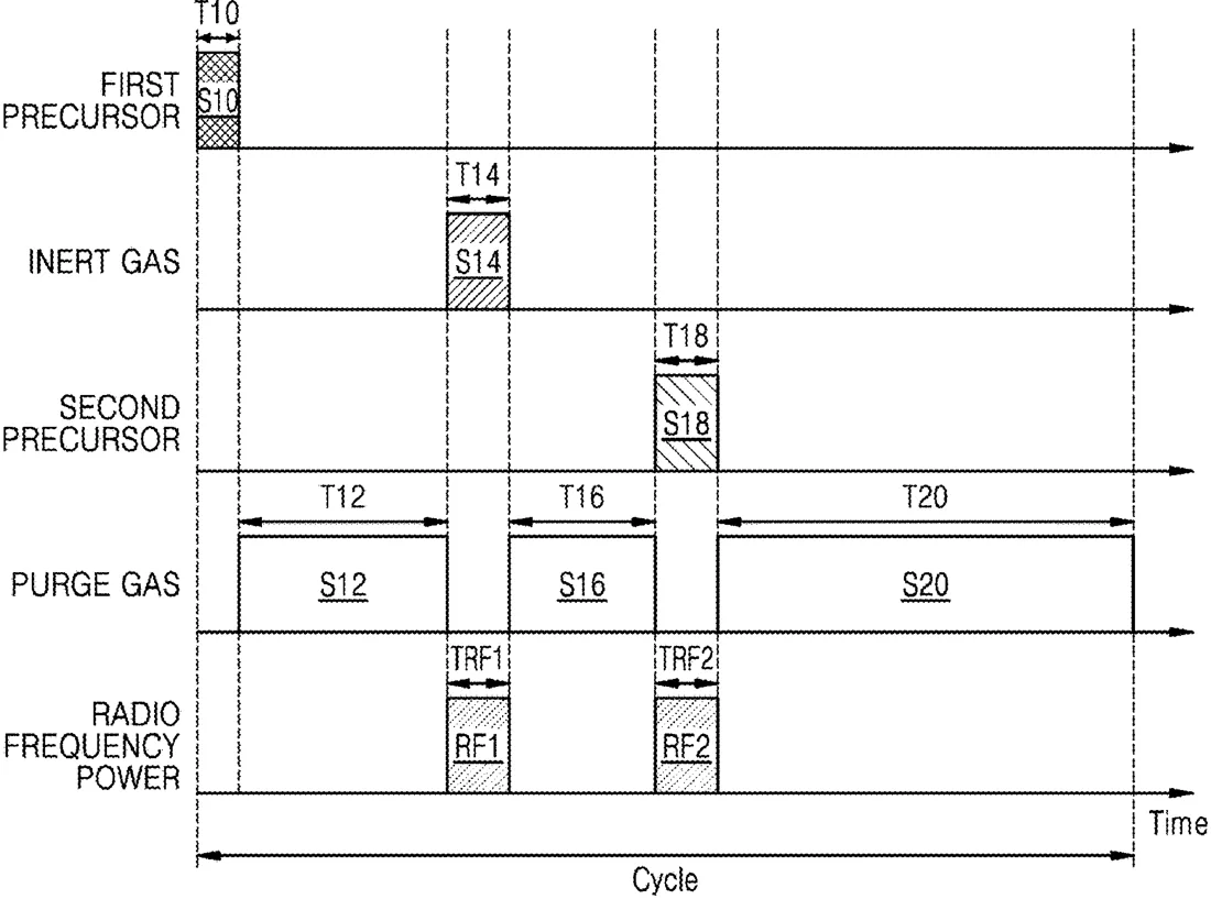
Samsung describes a specific sequence for building ultra-thin layers of material on chips using atomic layer deposition. The method involves alternating gas supplies and plasma treatments, with a key adjustment where one plasma step lasts longer than the initial gas supply step.
In the filing’s own words
A method of manufacturing a thin film by using an atomic layer deposition method including at least one cycle, and the at least one cycle includes forming a first adsorption layer onto a substrate for a first supply time, supplying a first purge gas onto the first adsorption layer for a first purge time, forming a second adsorption layer by supplying an inert gas in a plasma state onto the first adsorption layer for a second supply time, supplying a second purge gas onto the second adsorption layer for a second purge time, supplying a reactant gas in a plasma state onto the second adsorption layer for a third supply time to form a thin film, and supplying a third purge gas onto the thin film for a third purge time, in which the second supply time is longer than the first supply time.
What exactly they claim (claim 1)
1. A method of manufacturing a thin film by using an atomic layer deposition method including at least one cycle, wherein the at least one cycle includes: forming a first adsorption layer by supplying a metal precursor onto a substrate for a first supply time; supplying a first purge gas onto the first adsorption layer for a first purge time; forming a second adsorption layer by supplying an inert gas in a plasma state onto the first adsorption layer for a second supply time; supplying a second purge gas onto the second adsorption layer for a second purge time; supplying a reactant gas in a plasma state onto the second adsorption layer for a third supply time to allow the second adsorption layer to react with the reactant gas to form a thin film; and supplying a third purge gas onto the thin film for a third purge time, wherein the second supply time is longer than the first supply time.
Facts
- Company
- Samsung (SAMSUNG ELECTRONICS CO., LTD.)
- Official title
- METHOD OF MANUFACTURING THIN FILM BY USING ATOMIC LAYER DEPOSITION METHOD AND METHOD OF MANUFACTURING SEMICONDUCTOR DEVICE USING THE SAME
- Publication number
- US20260297746A1
- Application number
- 19576409
- Filed
- Mar 24, 2026
- Published
- Oct 1, 2026
- Inventors
- 3
- Claims
- 20
Classified under
C23C 16/4554 Chemistry & metalsC23C 16/4408 Chemistry & metalsC23C 16/45542 Chemistry & metalsC23C 16/45553 Chemistry & metalsC23C 16/505 Chemistry & metalsH10D 30/031 Electricity & electronicsMore from Samsung in Chips & hardware
- Samsung patents chip that combines camera and screen Oct 13, 2026
- Samsung patents faster chip testing using machine learning Sep 1, 2026
- Samsung patents radar method to pinpoint target direction more accurately Sep 1, 2026
- Samsung patents memory chip that searches data by content, not address Sep 1, 2026
- Samsung patents chip design that skips empty data to speed up AI Sep 1, 2026
Summaries are simplified from the filing’s own abstract and first claim. A patent filing is not a product announcement.
Patent data and drawings: U.S. Patent and Trademark Office (USPTO). Nebula is not affiliated with or endorsed by the USPTO.