Samsung patents method to flatten wavy silicon wafers
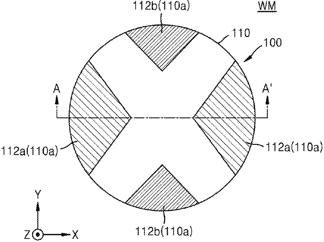
Samsung describes a method to measure how a silicon wafer bends or warps during manufacturing. The process uses a model to determine where to apply a stress-compensating film on the back of the wafer to counteract the bending.
In the filing’s own words
A warpage control method includes measuring displacement in a vertical direction perpendicular to a front surface of a wafer and dividing the front surface of the wafer into a first stress region with a negative displacement value and a second stress region with a positive displacement value, to thereby derive a warpage model, defining a portion of a region, overlapping the first stress region, on the front surface of the wafer as a first compensation region based on the warpage model and defining a region, other than the first compensation region, on the front surface of the wafer as a second compensation region based on the warpage model, to thereby derive a stress compensation film pattern model, and forming a mask pattern in a region on a back surface of the wafer.
What exactly they claim (claim 1)
1. A warpage control method comprising: measuring wafer displacement in a vertical direction perpendicular to a front surface of a wafer to identify that a first stress region of the front surface of the wafer has a negative displacement value, and that a second stress region of the front surface of the wafer has a positive displacement value; forming a mask pattern in a mask region on a back surface of the wafer, wherein the mask region overlaps a second compensation region on the front surface of the wafer in the vertical direction, wherein a first compensation region on the front surface of the wafer overlaps the first stress region in the vertical direction, and wherein the second compensation region comprises the front surface of the wafer other than the first compensation region; and depositing a stress compensation film over the mask region on the back surface and over at least a portion of the back surface other than the mask region.
Facts
- Company
- Samsung (SAMSUNG ELECTRONICS CO., LTD.)
- Official title
- Warpage control
- Patent number
- US12772853B2
- Application number
- 18632437
- Filed
- Apr 11, 2024
- Granted
- Oct 20, 2026
- Inventors
- 5
- Claims
- 20
Classified under
H10W 42/121 Electricity & electronicsH10P 74/203 Electricity & electronicsH10W 80/211 Electricity & electronicsH10W 80/312 Electricity & electronicsH10W 80/327 Electricity & electronicsMore from Samsung in Chips & hardware
- Samsung patents chip that combines camera and screen Oct 13, 2026
- Samsung patents faster chip testing using machine learning Sep 1, 2026
- Samsung patents radar method to pinpoint target direction more accurately Sep 1, 2026
- Samsung patents memory chip that searches data by content, not address Sep 1, 2026
- Samsung patents chip design that skips empty data to speed up AI Sep 1, 2026
Summaries are simplified from the filing’s own abstract and first claim. A patent filing is not a product announcement.
Patent data and drawings: U.S. Patent and Trademark Office (USPTO). Nebula is not affiliated with or endorsed by the USPTO.