Samsung patents chip with built-in liquid cooling channels
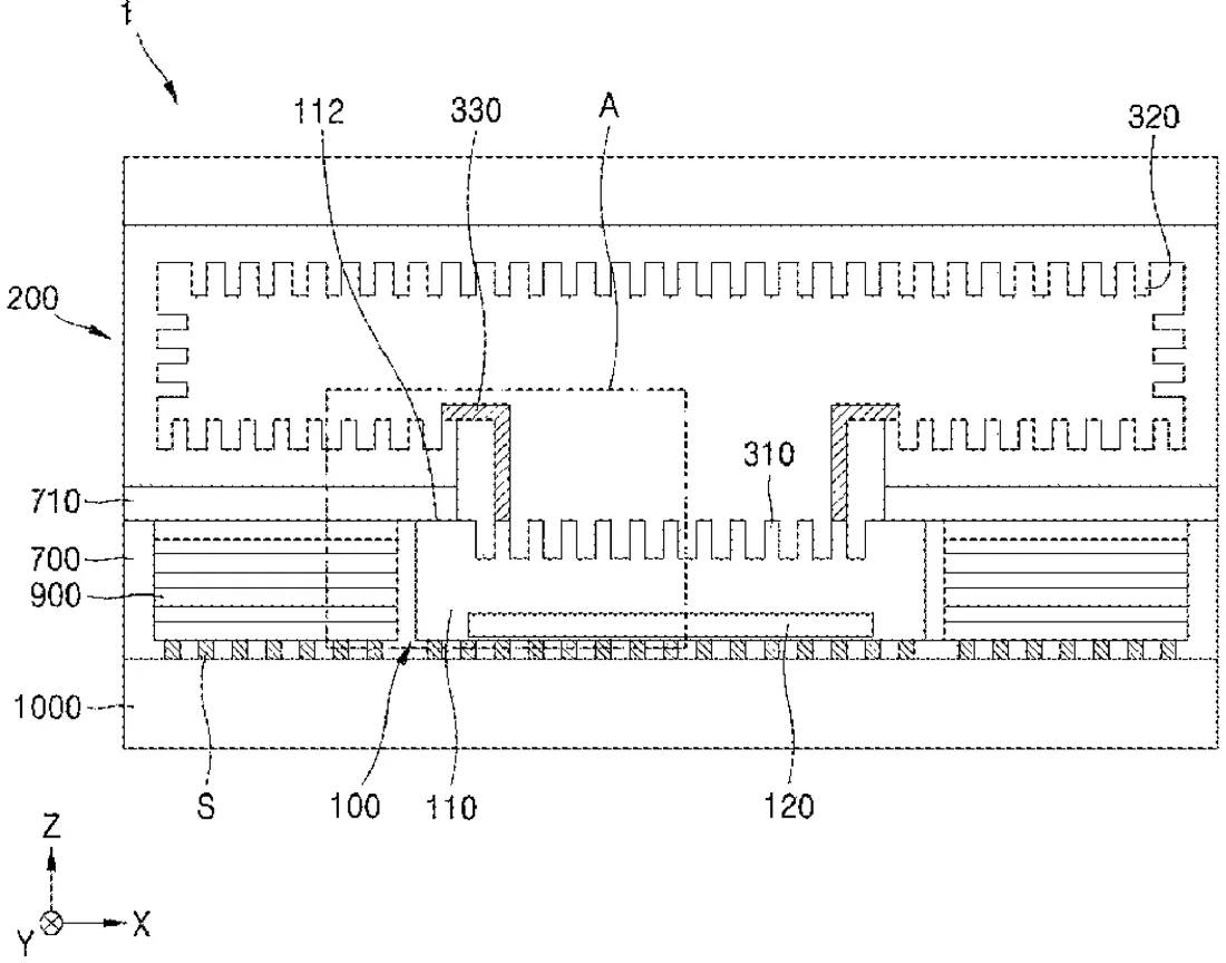
Samsung describes a semiconductor chip with a cooling channel carved directly into the silicon to absorb heat. Inside this channel, small textured structures called wicks use capillary action to move liquid coolant without a pump. A vapor chamber above the chip helps circulate the liquid to keep the processor cool.
In the filing’s own words
A semiconductor device includes a semiconductor chip having a semiconductor integrated circuit. A cooling channel is formed in the semiconductor chip. At least a portion of the cooling channel is formed in the semiconductor chip. First wick structures may be arranged on a bottom of the cooling channel that is parallel to an upper surface of the semiconductor chip in a transverse direction. The first wick structures may move a liquid coolant by capillary action in the transverse direction along the bottom of the cooling channel. Second wick structures may be arranged along an inner surface of the vapor chamber and may move the liquid coolant by capillary action in the transverse direction along the inner surface of the vapor chamber.
What exactly they claim (claim 1)
1. A semiconductor device comprising: a semiconductor chip including a cooling channel recessed in the semiconductor chip from an upper surface of the semiconductor chip, the cooling channel configured to have a liquid coolant flow therein such as to absorb heat generated during an operation of the semiconductor chip; first wick structures on a bottom of the cooling channel that is parallel to the upper surface of the semiconductor chip in a transverse direction, the first wick structures configured to move the liquid coolant by capillary action in the transverse direction along the bottom of the cooling channel; a vapor chamber above the semiconductor chip and in fluid communication with the cooling channel; second wick structures on an inner surface of the vapor chamber and configured to move the liquid coolant by capillary action in the transverse direction along the inner surface of the vapor chamber; and third wick structures between the first wick structures and the second wick structures and configured to move the liquid coolant from the second wick structures to the first wick structures by capillary action.
Facts
- Company
- Samsung (SAMSUNG ELECTRONICS CO., LTD.)
- Official title
- Semiconductor device
- Patent number
- US12772848B2
- Application number
- 18647903
- Filed
- Apr 26, 2024
- Granted
- Oct 20, 2026
- Inventors
- 5
- Claims
- 20
Classified under
H10W 40/47 Electricity & electronicsH10W 90/00 Electricity & electronicsMore from Samsung in Chips & hardware
- Samsung patents chip that combines camera and screen Oct 13, 2026
- Samsung patents faster chip testing using machine learning Sep 1, 2026
- Samsung patents radar method to pinpoint target direction more accurately Sep 1, 2026
- Samsung patents memory chip that searches data by content, not address Sep 1, 2026
- Samsung patents chip design that skips empty data to speed up AI Sep 1, 2026
Summaries are simplified from the filing’s own abstract and first claim. A patent filing is not a product announcement.
Patent data and drawings: U.S. Patent and Trademark Office (USPTO). Nebula is not affiliated with or endorsed by the USPTO.