Samsung patents laser-guided chip cleaning machine
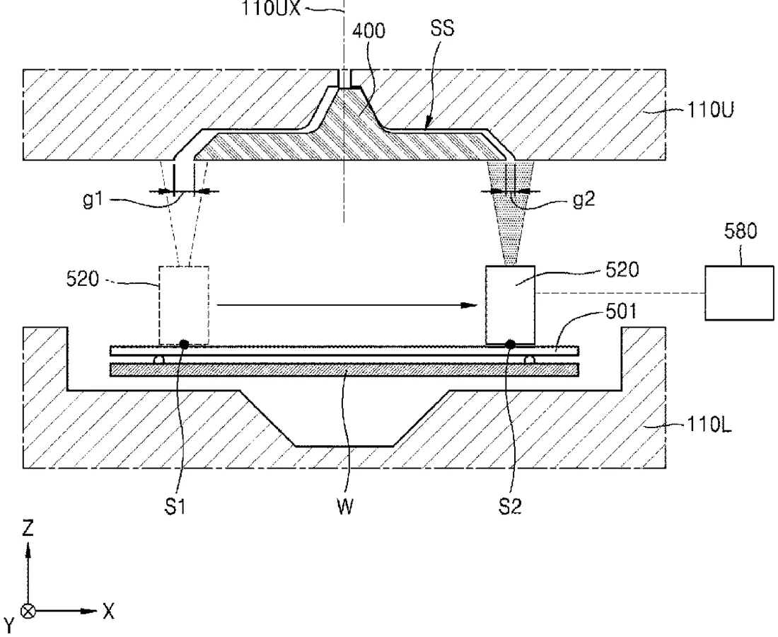
Samsung has been granted a patent for a machine that cleans semiconductor wafers using a special fluid. The device uses two laser sensors inside the chamber to check if the cleaning head is perfectly aligned with the wafer, then automatically adjusts the position to ensure even coverage.
In the filing’s own words
Provided is a substrate processing apparatus including a processing container having a processing space, a substrate support configured to support a substrate, a fluid supplier configured to supply a processing fluid in a supercritical state to the processing space, a shower head assembly configured to diffuse the processing fluid, a first laser portion configured to measure a horizontal alignment between the processing container and the shower head assembly, a second laser portion configured to measure a vertical alignment between the processing container and the shower head assembly, and a controller configured to correct the position of one of the substrate, the shower head assembly, and the processing container, based on the measured horizontal and vertical alignments, wherein the first and second laser portions are configured to be positioned within the processing container and to move above the substrate.
What exactly they claim (claim 1)
1. A substrate processing apparatus comprising: a processing container having a processing space; a substrate support configured to support a substrate in the processing container; a fluid supplier configured to supply a processing fluid in a supercritical state to the processing space through a container supply pipe; a shower head assembly configured to diffuse the processing fluid supplied from the fluid supplier into the processing space; a first laser portion configured to measure a horizontal alignment between the processing container and the shower head assembly; a second laser portion configured to measure a vertical alignment between the processing container and the shower head assembly; and a controller configured to correct a position of at least one of the substrate, the shower head assembly, and the processing container, based on the measured horizontal and vertical alignments, wherein the first laser portion and the second laser portion are configured to be positioned in the processing container and to move above the substrate.
Facts
- Company
- Samsung (Samsung Electronics Co., Ltd.)
- Official title
- Substrate processing apparatus and substrate processing method
- Patent number
- US12772782B2
- Application number
- 18520047
- Filed
- Nov 27, 2023
- Granted
- Oct 20, 2026
- Inventors
- 3
- Claims
- 17
Classified under
H10P 72/0606 Electricity & electronicsH10P 72/0402 Electricity & electronicsH10P 72/0431 Electricity & electronicsH10P 72/0462 Electricity & electronicsH10P 72/0604 Electricity & electronicsH10P 72/53 Electricity & electronicsMore from Samsung in Chips & hardware
- Samsung patents chip that combines camera and screen Oct 13, 2026
- Samsung patents faster chip testing using machine learning Sep 1, 2026
- Samsung patents radar method to pinpoint target direction more accurately Sep 1, 2026
- Samsung patents memory chip that searches data by content, not address Sep 1, 2026
- Samsung patents chip design that skips empty data to speed up AI Sep 1, 2026
Summaries are simplified from the filing’s own abstract and first claim. A patent filing is not a product announcement.
Patent data and drawings: U.S. Patent and Trademark Office (USPTO). Nebula is not affiliated with or endorsed by the USPTO.