Samsung patents chip design that mixes materials to control voltage
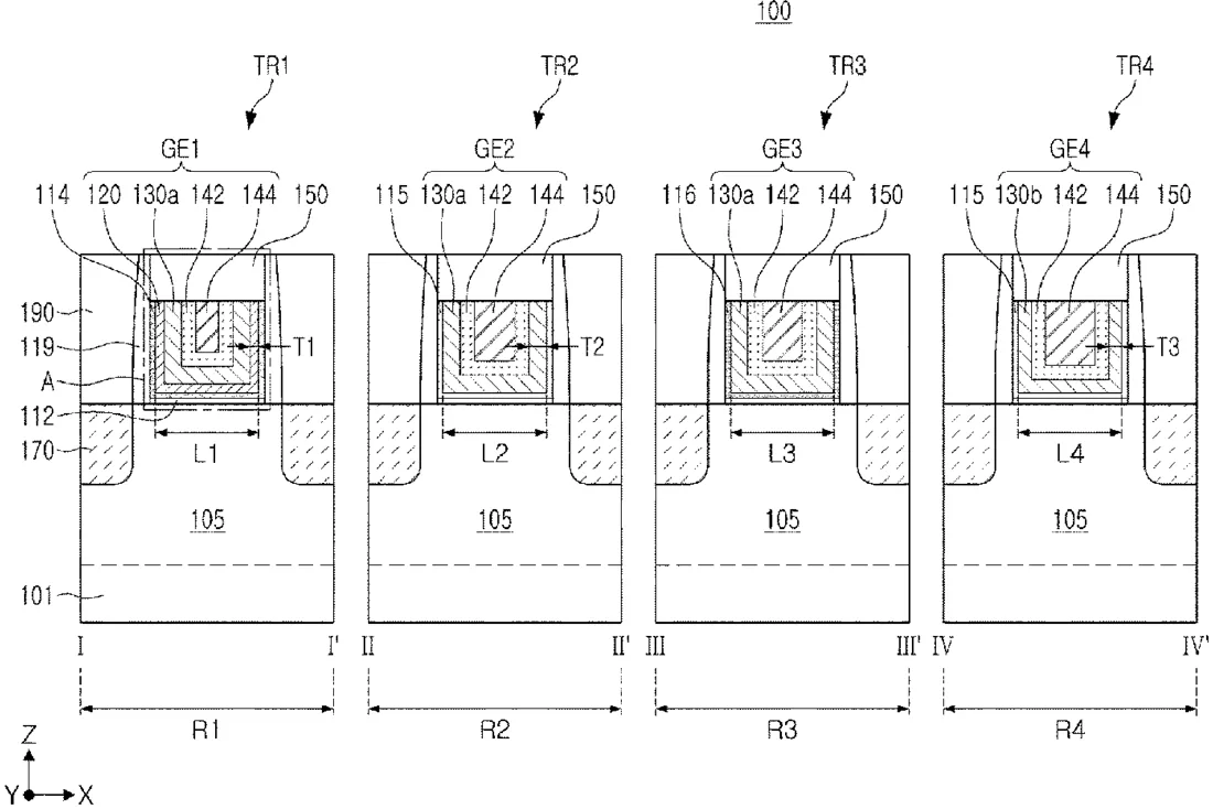
Samsung has been granted a patent for a semiconductor transistor design that uses different materials in specific regions of the chip. By adding specific elements to the gate dielectric layers, the design allows the transistor to operate at various voltages within the same device.
In the filing’s own words
A semiconductor device includes a substrate having a first, a second, a third, and a fourth region; a first gate structure in the first region and including a first gate dielectric layer, and a first, a second, and a third conductive layer; a second gate structure in the second region and including a second gate dielectric layer, and the second and the third conductive layer; a third gate structure in the third region and including a third gate dielectric layer, and the second and the third conductive layer; and a fourth gate structure in the fourth region and including the second gate dielectric layer, and a fourth and the third conductive layer. The first gate dielectric layer includes a material of the second gate dielectric layer and a first element, and the third gate dielectric layer includes a material of the second gate dielectric layer and a second element.
What exactly they claim (claim 1)
1. A semiconductor device comprising: a substrate comprising a first region and a second region; a first gate structure in the first region and comprising a first gate dielectric layer, a first conductive layer, a second conductive layer, and a third conductive layer, stacked in sequence; and a second gate structure in the second region and comprising a second gate dielectric layer, the second conductive layer, and the third conductive layer, stacked in sequence, wherein the first gate dielectric layer and the first conductive layer comprise a first element, and wherein the second conductive layer and the second gate dielectric layer are free of the first element, wherein the second gate dielectric layer is positioned on at least a first surface and a second surface of the second conductive layer, and wherein a first transistor comprising the first gate structure and a second transistor comprising the second gate structure define respective p-type MOSFETs.
Facts
- Company
- Samsung (Samsung Electronics Co., Ltd.)
- Official title
- Semiconductor transistors providing various operating voltages
- Patent number
- US12772536B2
- Application number
- 18743588
- Filed
- Jun 14, 2024
- Granted
- Oct 20, 2026
- Inventors
- 5
- Claims
- 11
Classified under
H10D 64/514 Electricity & electronicsH10D 64/519 Electricity & electronicsH10D 64/665 Electricity & electronicsH10D 84/014 Electricity & electronicsH10D 84/0144 Electricity & electronicsH10D 84/038 Electricity & electronicsMore from Samsung in Chips & hardware
- Samsung patents chip that combines camera and screen Oct 13, 2026
- Samsung patents faster chip testing using machine learning Sep 1, 2026
- Samsung patents radar method to pinpoint target direction more accurately Sep 1, 2026
- Samsung patents memory chip that searches data by content, not address Sep 1, 2026
- Samsung patents chip design that skips empty data to speed up AI Sep 1, 2026
Summaries are simplified from the filing’s own abstract and first claim. A patent filing is not a product announcement.
Patent data and drawings: U.S. Patent and Trademark Office (USPTO). Nebula is not affiliated with or endorsed by the USPTO.