Samsung patents 3D memory structure with bent internal wiring
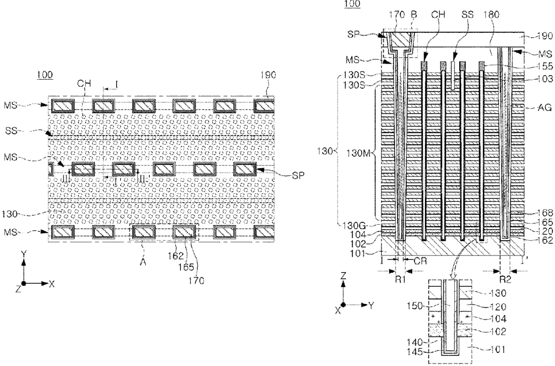
Samsung describes a design for vertical memory chips where internal wiring paths bend to connect different sections of the device. The filing details a specific layout for separating these paths and connecting them to the base material to improve the structure's stability.
In the filing’s own words
A semiconductor device includes a substrate, gate electrodes stacked in a first direction, channel structures penetrating through the gate electrodes, a horizontal conductive layer below the gate electrodes on the substrate, separation regions penetrating through the gate electrodes and the horizontal conductive layer, and extending in the first and second directions, a cell region insulating layer covering the gate electrodes, and an upper support layer on the separation regions and the cell region insulating layer and having openings to overlap the separation regions. Each of the separation regions includes a contact conductive layer and a first separation insulating layer in a trench, and has first regions below the openings and second regions alternating with the first regions. The contact conductive layer is in contact with the substrate in the first regions, and is spaced apart from the substrate by the first separation insulating layer in the second regions.
What exactly they claim (claim 1)
1. A semiconductor memory device, comprising: a substrate; gate electrodes stacked on the substrate, the gate electrodes being spaced apart from each other in a first direction perpendicular to an upper surface of the substrate; channel structures penetrating through the gate electrodes, the channel structures extending in the first direction and including channel layers, respectively; a horizontal conductive layer below the gate electrodes on the substrate, the horizontal conductive layer being in contact with the channel layers of the channel structures; separation regions penetrating through the gate electrodes and the horizontal conductive layer, the separation regions extending in the first direction and in a second direction perpendicular to the first direction, and the separation regions being spaced apart from each other in a third direction perpendicular to the first direction and the second direction; a cell region insulating layer covering the gate electrodes and the channel structures; an upper support layer on the separation regions and on the cell region insulating layer, the upper support layer having openings that overlap portions of the separation regions; and conductive pad layers in the openings, respectively, wherein each of the separation regions includes a contact conductive layer and a first separation insulating layer in a trench, and each of the separation regions has first regions below the openings and second regions alternating with the first regions, wherein the contact conductive layer is in contact with the substrate in the first regions, and is spaced apart from the substrate by the first separation insulating layer in the second regions, wherein each of the separation regions has a bent portion having a width in the third direction, wherein the width of the bent portion changes along the first direction below a corresponding one of the openings, wherein the bent portion is positioned at a higher vertical level than a vertical level of an uppermost gate electrode of the gate electrodes stacked on the substrate, wherein the conductive pad layers are connected to the contact conductive layer, and wherein for each of the separation regions, the bent portion and the uppermost gate electrode are separated by a gap.
Facts
- Company
- Samsung (SAMSUNG ELECTRONICS CO., LTD.)
- Official title
- Semiconductor devices including vertical common source line and data storage systems including the same
- Patent number
- US12772530B2
- Application number
- 17530651
- Filed
- Nov 19, 2021
- Granted
- Oct 20, 2026
- Inventors
- 3
- Claims
- 20
Classified under
H10D 64/111 Electricity & electronicsH10B 43/27 Electricity & electronicsH10W 20/20 Electricity & electronicsMore from Samsung in Chips & hardware
- Samsung patents chip that combines camera and screen Oct 13, 2026
- Samsung patents faster chip testing using machine learning Sep 1, 2026
- Samsung patents radar method to pinpoint target direction more accurately Sep 1, 2026
- Samsung patents memory chip that searches data by content, not address Sep 1, 2026
- Samsung patents chip design that skips empty data to speed up AI Sep 1, 2026
Summaries are simplified from the filing’s own abstract and first claim. A patent filing is not a product announcement.
Patent data and drawings: U.S. Patent and Trademark Office (USPTO). Nebula is not affiliated with or endorsed by the USPTO.