Samsung patents memory method that uses shared current to program cells
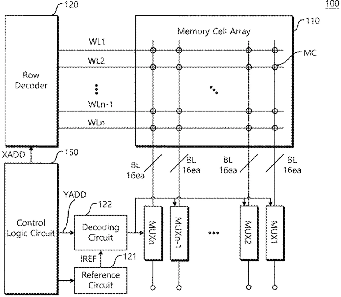
This patent describes a way to write data to memory chips by sending a specific current through multiple data lines at once. It uses a control system to adjust this current so that each line carries the exact amount needed to program the memory cells accurately.
In the filing’s own words
A memory device includes a memory cell array including a plurality of memory cells, respectively connected to a plurality of bitlines, a first multiplexer including a plurality of transistors connected to the plurality of bitlines, a reference circuit that generates reference current, a decoding circuit that transmits the reference current to the first multiplexer, and a control logic circuit connected to the reference circuit and the decoding circuit. The control logic circuit controls control the decoding circuit to apply the reference current to transistors, connected to each of at least two bitlines, such that predetermined first current flows through the at least two bitlines.
What exactly they claim (claim 1)
1. A memory device comprising: a memory cell array comprising a plurality of memory cells, respectively connected to a plurality of bitlines; a first multiplexer comprising a plurality of transistors connected to the plurality of bitlines; a reference circuit configured to generate a reference current; a decoding circuit comprising: a driver circuit comprising a digital logic; and a transmission circuit configured to transmit the reference current to the first multiplexer; and a control logic circuit configured to: control the decoding circuit to apply the reference current to at least two transistors among the plurality of transistors in the first multiplexer through the transmission circuit based on digital code output by the digital logic, the at least two transistors respectively connected to at least two bitlines among the plurality of bitlines.
Facts
- Company
- Samsung (SAMSUNG ELECTRONICS CO., LTD.)
- Official title
- Memory array programming method using bitlines and memory device for performing the same
- Patent number
- US12770693B2
- Application number
- 18753659
- Filed
- Jun 25, 2024
- Granted
- Oct 20, 2026
- Inventors
- 4
- Claims
- 17
Classified under
G11C 16/24 Physics & computingG11C 16/04 Physics & computingG11C 16/08 Physics & computingG11C 16/10 Physics & computingMore from Samsung in Chips & hardware
- Samsung patents chip that combines camera and screen Oct 13, 2026
- Samsung patents faster chip testing using machine learning Sep 1, 2026
- Samsung patents radar method to pinpoint target direction more accurately Sep 1, 2026
- Samsung patents memory chip that searches data by content, not address Sep 1, 2026
- Samsung patents chip design that skips empty data to speed up AI Sep 1, 2026
Summaries are simplified from the filing’s own abstract and first claim. A patent filing is not a product announcement.
Patent data and drawings: U.S. Patent and Trademark Office (USPTO). Nebula is not affiliated with or endorsed by the USPTO.