Samsung patents AI method to fix chip pattern errors during manufacturing
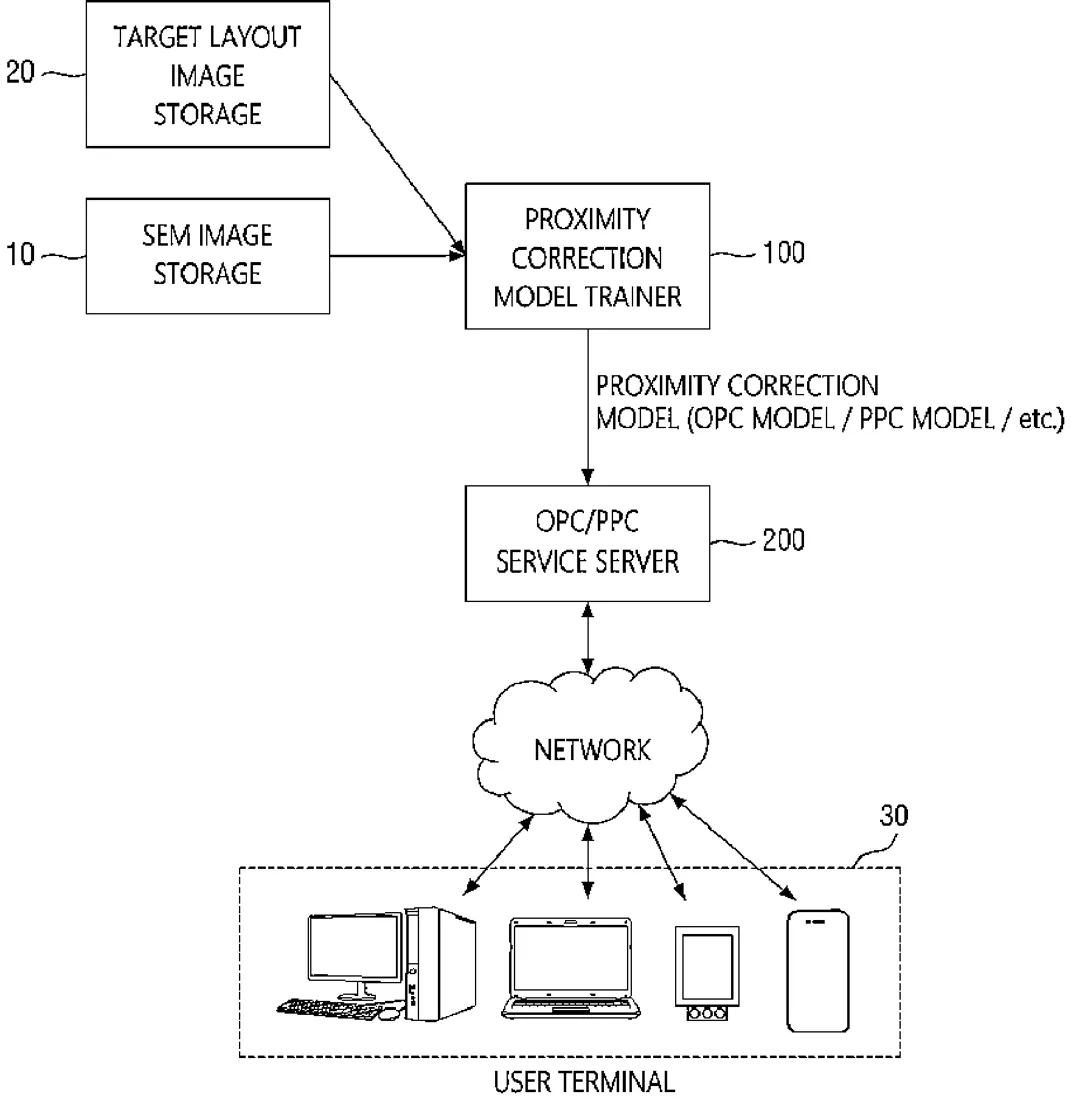
This patent describes a method for creating a model that predicts how patterns on a silicon wafer will look after a specific manufacturing step. It uses machine learning to compare the intended design with actual images of the wafer, accounting for how nearby patterns affect each other.
In the filing’s own words
A method for generating a proximity correction model which is performed by a computing system is provided. The method comprises acquiring a plurality of shot images on a wafer after performing a first process using a first layout, generating an overlap image obtained by overlap of the plurality of shot images, and performing machine learning on the proximity correction model, using an image of the first layout and the overlap image.
What exactly they claim (claim 1)
1. A method for generating a proximity correction model which is performed by a computing system, the method comprising: acquiring a plurality of shot images of a wafer after performing a first process on the wafer using a first layout; generating an overlap image, the overlap image obtained by overlapping the plurality of shot images; and performing machine learning on the proximity correction model such that the proximity correction model is configured to generate a predicted image of a pattern formed after performing the first process using a target layout, the performing the machine learning including using training data including an image of the first layout and the overlap image, wherein the generating the overlap image comprises extracting contours of each of plurality of shot images, dithering the extracted contours of each of the plurality of shot images, and generating the overlap image by overlapping the dithered contours of each of the plurality of shot images.
Facts
- Company
- Samsung (Samsung Electronics Co., Ltd.)
- Official title
- Method for generating proximity correction model, method for processing proximity correction using generated proximity correction model and proximity correction system thereof
- Patent number
- US12770249B2
- Application number
- 18631579
- Filed
- Apr 10, 2024
- Granted
- Oct 20, 2026
- Inventors
- 2
- Claims
- 19
Classified under
G06T 7/001 Physics & computingG06T 2207/20081 Physics & computingG06T 2207/30148 Physics & computingMore from Samsung in Chips & hardware
- Samsung patents chip that combines camera and screen Oct 13, 2026
- Samsung patents faster chip testing using machine learning Sep 1, 2026
- Samsung patents radar method to pinpoint target direction more accurately Sep 1, 2026
- Samsung patents memory chip that searches data by content, not address Sep 1, 2026
- Samsung patents chip design that skips empty data to speed up AI Sep 1, 2026
Summaries are simplified from the filing’s own abstract and first claim. A patent filing is not a product announcement.
Patent data and drawings: U.S. Patent and Trademark Office (USPTO). Nebula is not affiliated with or endorsed by the USPTO.