Samsung patents memory system that speeds up AI data lookups
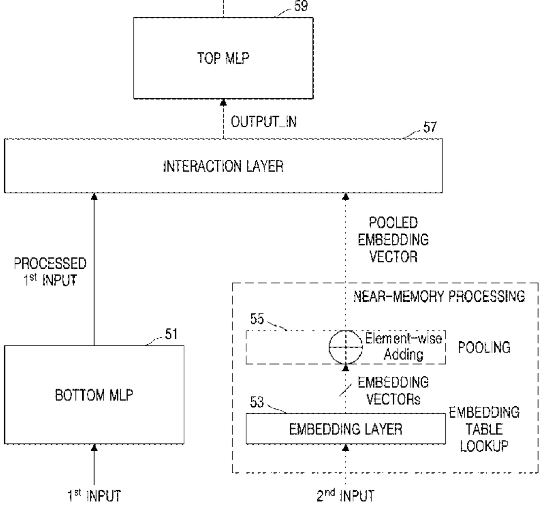
Samsung has patented a memory design that splits data storage into two parts to handle large sets of AI data, known as embedding vectors. It keeps frequently used data in a fast, local buffer while storing the rest in a compressed form in slower memory, decompressing it only when needed.
In the filing’s own words
A memory device including a near-memory device and a far-memory device, wherein the far-memory device stores compressed embedding vectors, the near-memory device including: a buffer to receive a request for pooling an embedding vector and output a hit or miss signal in response to the request, wherein the hit signal includes the embedding vector corresponding to the request; an address calculation circuit to calculate a starting memory address and memory size of the embedding vector in response to the miss signal; a decoding circuit to obtain a compressed embedding vector corresponding to the request from the far-memory device based on the starting memory address and memory size, and output the embedding vector corresponding to the request by decoding the compressed embedding vector; and a pooling circuit to output a pooled embedding vector by performing a pooling operation on the embedding vector.
What exactly they claim (claim 1)
1. A memory device comprising a near-memory device and a far-memory device, wherein the far-memory device stores compressed embedding vectors, the near-memory device comprising: a buffer configured to receive a request for pooling an embedding vector and to output a hit signal or a miss signal in response to the request, wherein the hit signal includes the embedding vector corresponding to the request; an address calculation circuit configured to calculate a starting memory address and a memory size of the embedding vector corresponding to the request in response to the miss signal; a decoding circuit configured to obtain a compressed embedding vector corresponding to the request from the far-memory device based on the starting memory address and the memory size, and to output the embedding vector corresponding to the request by decoding the compressed embedding vector; and a pooling circuit configured to output a pooled embedding vector by performing a pooling operation on the embedding vector, wherein the pooling circuit obtains the embedding vector from the hit signal or obtains the embedding vector from the decoding circuit, and the buffer stores embedding vectors with access frequencies higher than a pre-set value from all embedding vectors.
Facts
- Company
- Samsung (SAMSUNG ELECTRONICS CO., LTD.)
- Official title
- Near memory device, memory device, and electronic device
- Patent number
- US12769656B2
- Application number
- 19013254
- Filed
- Jan 8, 2025
- Granted
- Oct 20, 2026
- Inventors
- 2
- Claims
- 20
Classified under
G06F 12/06 Physics & computingMore from Samsung in Chips & hardware
- Samsung patents chip that combines camera and screen Oct 13, 2026
- Samsung patents faster chip testing using machine learning Sep 1, 2026
- Samsung patents radar method to pinpoint target direction more accurately Sep 1, 2026
- Samsung patents memory chip that searches data by content, not address Sep 1, 2026
- Samsung patents chip design that skips empty data to speed up AI Sep 1, 2026
Summaries are simplified from the filing’s own abstract and first claim. A patent filing is not a product announcement.
Patent data and drawings: U.S. Patent and Trademark Office (USPTO). Nebula is not affiliated with or endorsed by the USPTO.