Samsung patents circuit that merges two clock signals into one
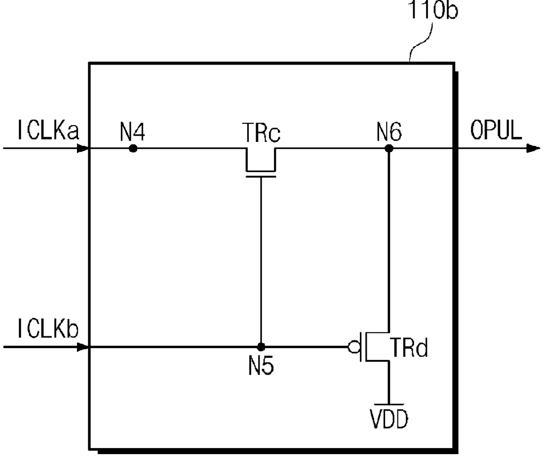
This filing describes a circuit that combines two clock signals with the same speed but different timing into a single output pulse. It uses transistors to switch between the two inputs based on their logic levels to create a continuous signal.
In the filing’s own words
Disclosed is a clock multiplexing circuit which includes a first transistor that is between a first input terminal that receives a first input clock signal and an output terminal that outputs an output pulse signal and operates based on a logic level of a second input terminal receiving a second input clock signal, and a second transistor that is between the output terminal and a first voltage node and operates based on the logic level of the second input terminal. The first input clock signal and the second input clock signal have the same period and have different phases. The output pulse signal transitions to a first logic level at a first time when the first input clock signal transitions to the first logic level and transitions to a second logic level at a second time when the second input clock signal transitions to the first logic level.
What exactly they claim (claim 1)
1. A clock multiplexing circuit comprising: a first transistor that is between a first input terminal that is configured to receive a first input clock signal and an output terminal that is configured to output an output pulse signal, wherein the first transistor is configured to be turned on to electrically connect the first input terminal and the output terminal in response to a logic level of a second input terminal that is configured to receive a second input clock signal being a first logic level; and a second transistor that is between the output terminal and a first voltage node, wherein the second transistor is configured to be turned on to electrically connect the first voltage node and the output terminal in response to the logic level of the second input terminal being a second logic level different from the first logic level, wherein the first input clock signal and the second input clock signal have a same period and have different phases.
Facts
- Company
- Samsung (Samsung Electronics Co., Ltd.)
- Official title
- Clock multiplexing circuit
- Patent number
- US12769358B2
- Application number
- 18922797
- Filed
- Oct 22, 2024
- Granted
- Oct 20, 2026
- Inventors
- 4
- Claims
- 20
Classified under
G06F 1/12 Physics & computingMore from Samsung in Chips & hardware
- Samsung patents chip that combines camera and screen Oct 13, 2026
- Samsung patents faster chip testing using machine learning Sep 1, 2026
- Samsung patents radar method to pinpoint target direction more accurately Sep 1, 2026
- Samsung patents memory chip that searches data by content, not address Sep 1, 2026
- Samsung patents chip design that skips empty data to speed up AI Sep 1, 2026
Summaries are simplified from the filing’s own abstract and first claim. A patent filing is not a product announcement.
Patent data and drawings: U.S. Patent and Trademark Office (USPTO). Nebula is not affiliated with or endorsed by the USPTO.