Samsung patents method for detecting wafer mark coordinates
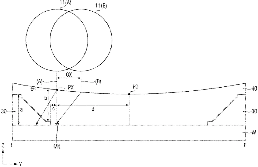
Samsung has been granted a patent for a method to detect the precise location of a reference mark on a silicon wafer during chip manufacturing. The technique involves creating specific stacked structures with stair-shaped ends around the mark and using a beam to measure its position. It then calculates and corrects for any shifts in the beam's path to ensure accurate alignment.
In the filing’s own words
A method of detecting coordinates of a mark is provided. The method includes: providing a plurality of structures and the mark on a wafer, each of the plurality of structures including a plurality of mold insulating layers and a plurality of mold sacrificial layers, which are alternately stacked, an end of each of the plurality of structures including a portion having a stair shape, and the mark being between adjacent structures among the plurality of structures; forming a photoresist layer on the plurality of structures and the mark, the photoresist layer including a portion concave toward the wafer between the adjacent structures; detecting the coordinates of the mark by irradiating a beam to the mark; determining an offset of the coordinates of the mark based on a beam path changing factor; and correcting the coordinates of the mark based on the offset.
What exactly they claim (claim 1)
1. A method of detecting coordinates of a mark, the method comprising: providing a plurality of structures and the mark on a wafer, each of the plurality of structures comprising a plurality of mold insulating layers and a plurality of mold sacrificial layers, which are alternately stacked, an end of each of the plurality of structures comprising a portion having a stair shape, and the mark being between adjacent structures among the plurality of structures; forming a photoresist layer on the plurality of structures and the mark, the photoresist layer comprising a portion concave toward the wafer between the adjacent structures; detecting the coordinates of the mark by irradiating a beam to the mark; determining an offset of the coordinates of the mark based on a beam path changing factor; and correcting the coordinates of the mark based on the offset.
Facts
- Company
- Samsung (Samsung Electronics Co., Ltd.)
- Official title
- Method for detecting coordinate of mark, computing system for performing the same, and lithography method
- Patent number
- US12769220B2
- Application number
- 18233083
- Filed
- Aug 11, 2023
- Granted
- Oct 20, 2026
- Inventors
- 3
- Claims
- 16
Classified under
G03F 9/7088 Physics & computingG03F 7/039 Physics & computingG03F 7/70625 Physics & computingG03F 7/70683 Physics & computingG03F 7/706849 Physics & computingMore from Samsung in Chips & hardware
- Samsung patents chip that combines camera and screen Oct 13, 2026
- Samsung patents faster chip testing using machine learning Sep 1, 2026
- Samsung patents radar method to pinpoint target direction more accurately Sep 1, 2026
- Samsung patents memory chip that searches data by content, not address Sep 1, 2026
- Samsung patents chip design that skips empty data to speed up AI Sep 1, 2026
Summaries are simplified from the filing’s own abstract and first claim. A patent filing is not a product announcement.
Patent data and drawings: U.S. Patent and Trademark Office (USPTO). Nebula is not affiliated with or endorsed by the USPTO.