Samsung patents new chemical mix for making finer computer chips
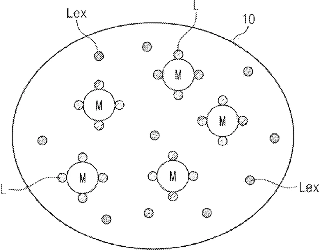
Samsung describes a specific chemical mixture used to create photoresist, a light-sensitive material needed to etch patterns onto silicon wafers. The formula combines a metal compound with two extra chemical parts that have different shapes and properties to help control how the material reacts to light during chip manufacturing.
In the filing’s own words
A resist composition and a method of manufacturing a semiconductor device, the resist composition includes an organometallic compound, the organometallic compound including a central metal and ligands combined with the central metal; and an excess ligand compound, the excess ligand compound being combinable with the central metal via a coordination bond.
What exactly they claim (claim 1)
1. A method of manufacturing a semiconductor device, the method comprising: forming a photoresist layer by applying a resist composition on a lower layer; and performing an exposure process on the photoresist layer, wherein the resist composition includes: an organometallic compound, the organometallic compound including a central metal and ligands combined with the central metal; and an excess ligand compound comprising a first excess ligand and a second excess ligand that are not combined with any central metal, wherein the first excess ligand and the second excess ligand have different functional groups from each other, wherein a bulkiness of the first excess ligand is different from a bulkiness of the second excess ligand.
Facts
- Company
- Samsung (SAMSUNG ELECTRONICS CO., LTD.)
- Official title
- Resist composition and method of manufacturing semiconductor device using the same
- Patent number
- US12769203B2
- Application number
- 18127118
- Filed
- Mar 28, 2023
- Granted
- Oct 20, 2026
- Inventors
- 4
- Claims
- 14
Classified under
G03F 7/0042 Physics & computingH10P 76/2041 Electricity & electronicsMore from Samsung in Chips & hardware
- Samsung patents chip that combines camera and screen Oct 13, 2026
- Samsung patents faster chip testing using machine learning Sep 1, 2026
- Samsung patents radar method to pinpoint target direction more accurately Sep 1, 2026
- Samsung patents memory chip that searches data by content, not address Sep 1, 2026
- Samsung patents chip design that skips empty data to speed up AI Sep 1, 2026
Summaries are simplified from the filing’s own abstract and first claim. A patent filing is not a product announcement.
Patent data and drawings: U.S. Patent and Trademark Office (USPTO). Nebula is not affiliated with or endorsed by the USPTO.