Samsung patents method using polyurea to selectively grow films on chips
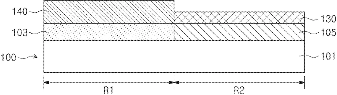
This patent describes a manufacturing process for creating thin layers on electronic components. It uses a temporary polyurea coating to protect specific areas of a substrate while a target film is grown on other exposed areas.
In the filing’s own words
An area-selective film forming method may include preparing a substrate having at least two areas made of different materials, forming a polyurea film on the at least two areas of the substrate, annealing the polyurea film and selectively removing the polyurea film on at least one area among the at least two areas, and forming a target film on the one area or a remaining area among the at least two areas. The one area may be an area from which the polyurea film is removed. The remaining area may be an area in which the polyurea film is not removed during the annealing the polyurea film and the selectively removing the polyurea film.
What exactly they claim (claim 1)
1. An area-selective film forming method comprising: preparing a substrate having a first area and a second area, the first area and the second area being made of different materials; forming a polyurea film on the first area and the second area; annealing the polyurea film and selectively removing the polyurea film from the second area to form a polyurea film pattern on the first area, wherein a thickness of the polyurea film pattern is smaller than a thickness of the polyurea film on the first area; selectively forming a layer forming inhibitor on the second area from which the polyurea film is removed; removing the polyurea film pattern on the first area; forming a target film on the first area, wherein a thickness of the target film is greater than a thickness of the layer forming inhibitor; and removing the layer forming inhibitor on the second area.
Facts
- Company
- Samsung (Samsung Electronics Co., Ltd.)
- Official title
- Area-selective film forming method using polyurea
- Patent number
- US12768032B2
- Application number
- 18753418
- Filed
- Jun 25, 2024
- Granted
- Oct 20, 2026
- Inventors
- 10
- Claims
- 18
Classified under
C23C 16/042 Chemistry & metalsB05D 1/60 Operations & transportC23C 16/0272 Chemistry & metalsC23C 16/06 Chemistry & metalsMore from Samsung in Chips & hardware
- Samsung patents chip that combines camera and screen Oct 13, 2026
- Samsung patents faster chip testing using machine learning Sep 1, 2026
- Samsung patents radar method to pinpoint target direction more accurately Sep 1, 2026
- Samsung patents memory chip that searches data by content, not address Sep 1, 2026
- Samsung patents chip design that skips empty data to speed up AI Sep 1, 2026
Summaries are simplified from the filing’s own abstract and first claim. A patent filing is not a product announcement.
Patent data and drawings: U.S. Patent and Trademark Office (USPTO). Nebula is not affiliated with or endorsed by the USPTO.