Samsung patents semiconductor wiring layout for tighter chip connections
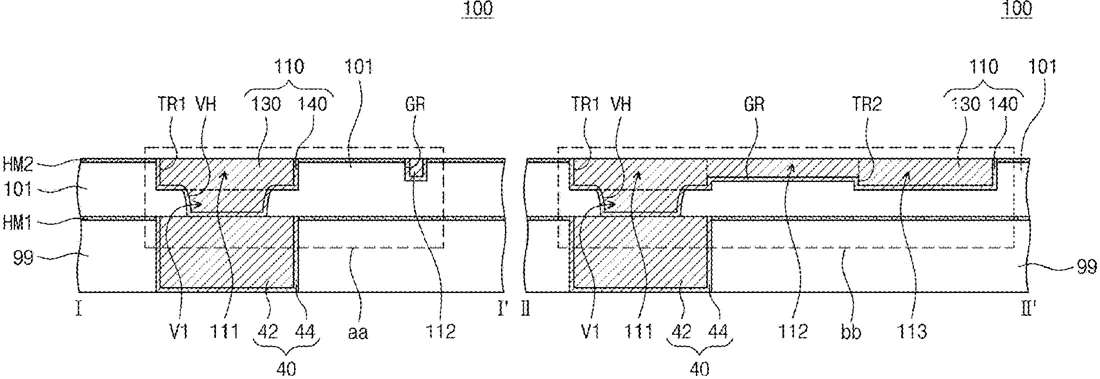
Samsung has been granted a patent for a specific way to build the tiny electrical connections inside a semiconductor package. The design uses a protective layer to carve out holes and trenches, then fills them with metal to create a connected path that includes a vertical drop, a flat pad, and a horizontal line. This structure allows the wiring to be packed more tightly by using materials that react differently during the etching process.
In the filing’s own words
Disclosed are interconnection structures and semiconductor packages. The interconnection structure includes a first dielectric layer and a first hardmask pattern that are sequentially stacked, and a first interconnection pattern that penetrates the first hardmask pattern and the first dielectric layer. The first hardmask pattern includes a dielectric material having an etch selectivity with respect to the first dielectric layer. The first interconnection pattern includes a via part, a first pad part, and a line part that are integrally connected to each other. The first pad part vertically overlaps the via part. The line part extends from the first pad part. A level of a bottom surface of the first pad part is lower than a level of a bottom surface of the line part.
What exactly they claim (claim 1)
1. A method of manufacturing an interconnection structure, comprising: providing a dielectric layer; forming a hardmask layer including a dielectric material having an etch selectivity with respect to the dielectric layer and covering an upper surface of the dielectric layer; forming a hardmask pattern by etching the hardmask layer with a mask pattern; forming a via hole and trenches in the dielectric layer by etching the dielectric layer using the mask pattern and the hardmask pattern as masks; and forming an interconnection pattern covering the via hole and the trenches, wherein the interconnection pattern includes a via part covering the via hole, a pad part vertically overlapping the via part, and a line part extending from the pad part, and wherein a bottom surface of the pad part, a bottom surface of the line part, and a lateral surface of the via part are in contact with the dielectric layer, wherein the via hole and the trenches are defined by the dielectric layer such that the dielectric layer surrounds the via part, the pad part, and the line part in a lateral direction, and wherein the dielectric layer is a single dielectric layer.
Facts
- Company
- Samsung (Samsung Electronics Co., Ltd.)
- Official title
- Interconnection structure and semiconductor package including the same
- Patent number
- US12765409B2
- Application number
- 18655879
- Filed
- May 6, 2024
- Granted
- Oct 13, 2026
- Inventors
- 6
- Claims
- 20
Classified under
H10W 70/685 Electricity & electronicsH10W 70/611 Electricity & electronicsH10W 70/614 Electricity & electronicsH10W 70/65 Electricity & electronicsH10W 74/117 Electricity & electronicsH10W 90/00 Electricity & electronicsMore from Samsung in Chips & hardware
- Samsung patents chip that combines camera and screen Oct 13, 2026
- Samsung patents faster chip testing using machine learning Sep 1, 2026
- Samsung patents radar method to pinpoint target direction more accurately Sep 1, 2026
- Samsung patents memory chip that searches data by content, not address Sep 1, 2026
- Samsung patents chip design that skips empty data to speed up AI Sep 1, 2026
Summaries are simplified from the filing’s own abstract and first claim. A patent filing is not a product announcement.
Patent data and drawings: U.S. Patent and Trademark Office (USPTO). Nebula is not affiliated with or endorsed by the USPTO.