Samsung patents chip layout with uneven transistor spacing
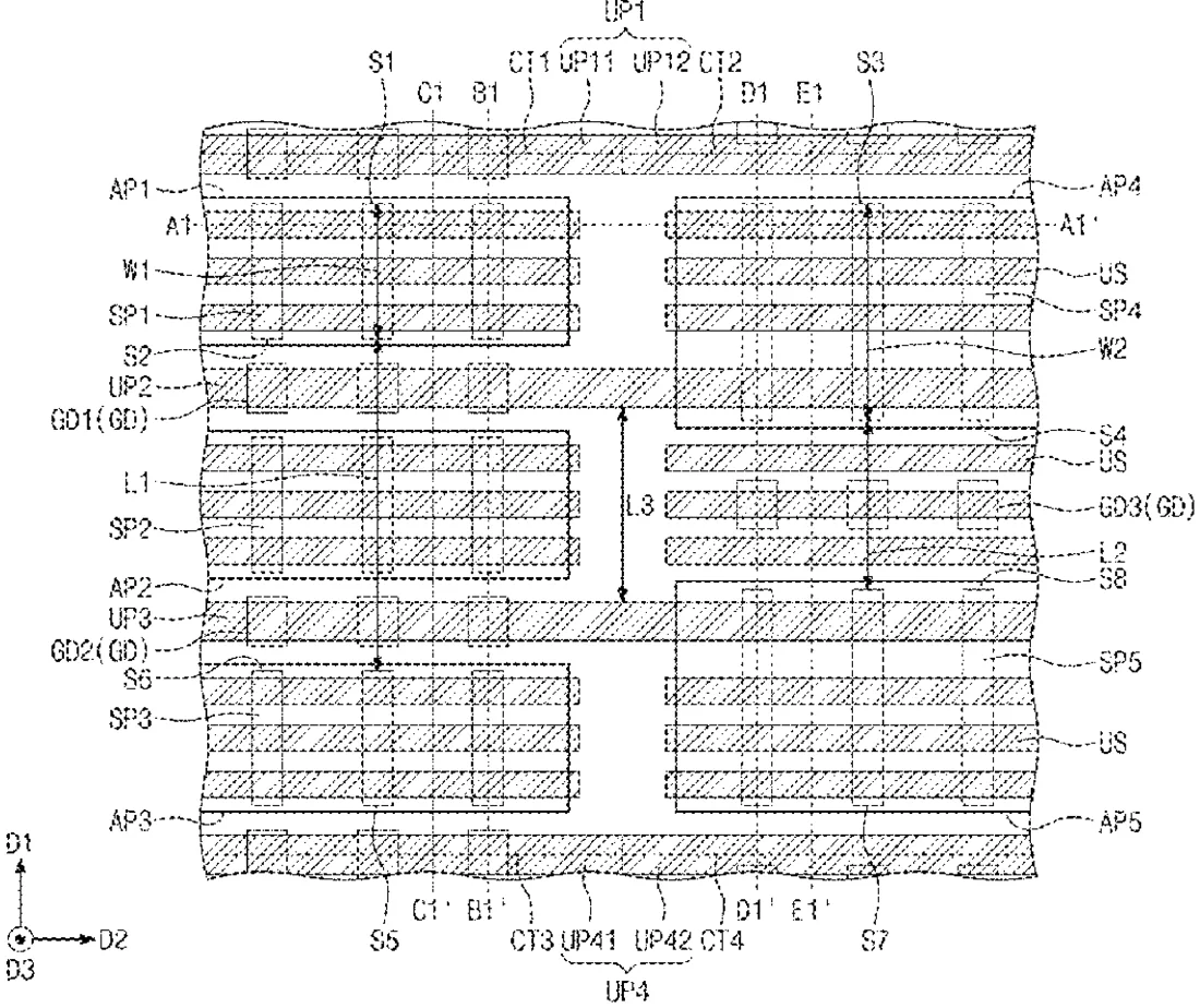
Samsung has been granted a patent for a specific arrangement of transistors and power lines within a semiconductor chip. The design places five transistor patterns between two power lines, with the middle transistor spaced further from its neighbors than the outer transistors are from each other.
In the filing’s own words
Disclosed is a semiconductor device comprising a first upper power line and a second upper power line extending in a first direction and are spaced apart from each other in a second direction intersecting the first direction, a first semiconductor pattern, a second semiconductor pattern spaced apart in the second direction from the first semiconductor pattern, a third semiconductor pattern spaced apart in the second direction from the second semiconductor pattern, a fourth semiconductor pattern spaced apart in the first direction from the first semiconductor pattern, and a fifth semiconductor pattern spaced apart in the first direction from the third semiconductor pattern. The first to fifth semiconductor patterns are between the first upper power line and the second upper power line. The second semiconductor pattern is between the first semiconductor pattern and the third semiconductor pattern.
What exactly they claim (claim 1)
1. A semiconductor device, comprising: a first upper power line and a second upper power line extending in a first direction and are spaced apart from each other in a second direction intersecting the first direction; a first semiconductor pattern; a second semiconductor pattern spaced apart in the second direction from the first semiconductor pattern; a third semiconductor pattern spaced apart in the second direction from the second semiconductor pattern; a fourth semiconductor pattern spaced apart in the first direction from the first semiconductor pattern; and a fifth semiconductor pattern spaced apart in the first direction from the third semiconductor pattern, wherein the first to fifth semiconductor patterns are between the first upper power line and the second upper power line, wherein the second semiconductor pattern is between the first semiconductor pattern and the third semiconductor pattern, and wherein a distance between the first semiconductor pattern and the third semiconductor pattern is greater than a distance between the fourth semiconductor pattern and the fifth semiconductor pattern.
Facts
- Company
- Samsung (Samsung Electronics Co., Ltd.)
- Official title
- Semiconductor device
- Patent number
- US12765358B2
- Application number
- 18641525
- Filed
- Apr 22, 2024
- Granted
- Oct 13, 2026
- Inventors
- 4
- Claims
- 20
Classified under
H10W 20/427 Electricity & electronicsH10D 30/43 Electricity & electronicsH10D 30/6729 Electricity & electronicsH10D 30/6735 Electricity & electronicsH10D 30/6757 Electricity & electronicsH10D 62/121 Electricity & electronicsMore from Samsung in Chips & hardware
- Samsung patents chip that combines camera and screen Oct 13, 2026
- Samsung patents faster chip testing using machine learning Sep 1, 2026
- Samsung patents radar method to pinpoint target direction more accurately Sep 1, 2026
- Samsung patents memory chip that searches data by content, not address Sep 1, 2026
- Samsung patents chip design that skips empty data to speed up AI Sep 1, 2026
Summaries are simplified from the filing’s own abstract and first claim. A patent filing is not a product announcement.
Patent data and drawings: U.S. Patent and Trademark Office (USPTO). Nebula is not affiliated with or endorsed by the USPTO.