Samsung patents chip design that uses laser heat to test for defects
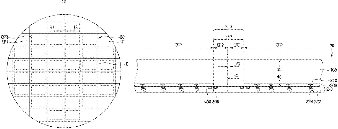
This patent describes a semiconductor chip with special test areas built into the unused space around the main circuit. These areas contain tiny circuits that produce a small electrical leak when hit by a laser, allowing engineers to check if the chip is working correctly during manufacturing.
In the filing’s own words
A semiconductor chip includes a semiconductor substrate having a first surface and a second surface opposite to the first surface. The semiconductor substrate includes a circuit pattern region and a peripheral region surrounding the circuit pattern region, an activation layer on the second surface of the semiconductor substrate and having a plurality of circuit patterns in the circuit pattern region, and at least one scattering detection pattern in the peripheral region and having a plurality of circuit cells that generate leakage current based on a scattered beam or heat of a laser.
What exactly they claim (claim 1)
1. A semiconductor chip, comprising: a semiconductor substrate having a first surface and a second surface opposite to the first surface, the semiconductor substrate including a circuit pattern region and a peripheral region surrounding the circuit pattern region; an activation layer on the second surface of the semiconductor substrate, the activation layer having a plurality of circuit patterns in the circuit pattern region; and at least one scattering detection pattern in the peripheral region, the at least one scattering detection pattern having a plurality of circuit cells configured to generate a leakage current based on a scattered beam or heat of a laser.
Facts
- Company
- Samsung (Samsung Electronics Co., Ltd.)
- Official title
- Semiconductor chip, semiconductor device including semiconductor chips, and method of inspecting the semiconductor device
- Patent number
- US12765329B2
- Application number
- 18635180
- Filed
- Apr 15, 2024
- Granted
- Oct 13, 2026
- Inventors
- 4
- Claims
- 20
Classified under
H10P 74/277 Electricity & electronicsMore from Samsung in Chips & hardware
- Samsung patents chip that combines camera and screen Oct 13, 2026
- Samsung patents faster chip testing using machine learning Sep 1, 2026
- Samsung patents radar method to pinpoint target direction more accurately Sep 1, 2026
- Samsung patents memory chip that searches data by content, not address Sep 1, 2026
- Samsung patents chip design that skips empty data to speed up AI Sep 1, 2026
Summaries are simplified from the filing’s own abstract and first claim. A patent filing is not a product announcement.
Patent data and drawings: U.S. Patent and Trademark Office (USPTO). Nebula is not affiliated with or endorsed by the USPTO.