Samsung patents laser method to crack wafers for chip separation
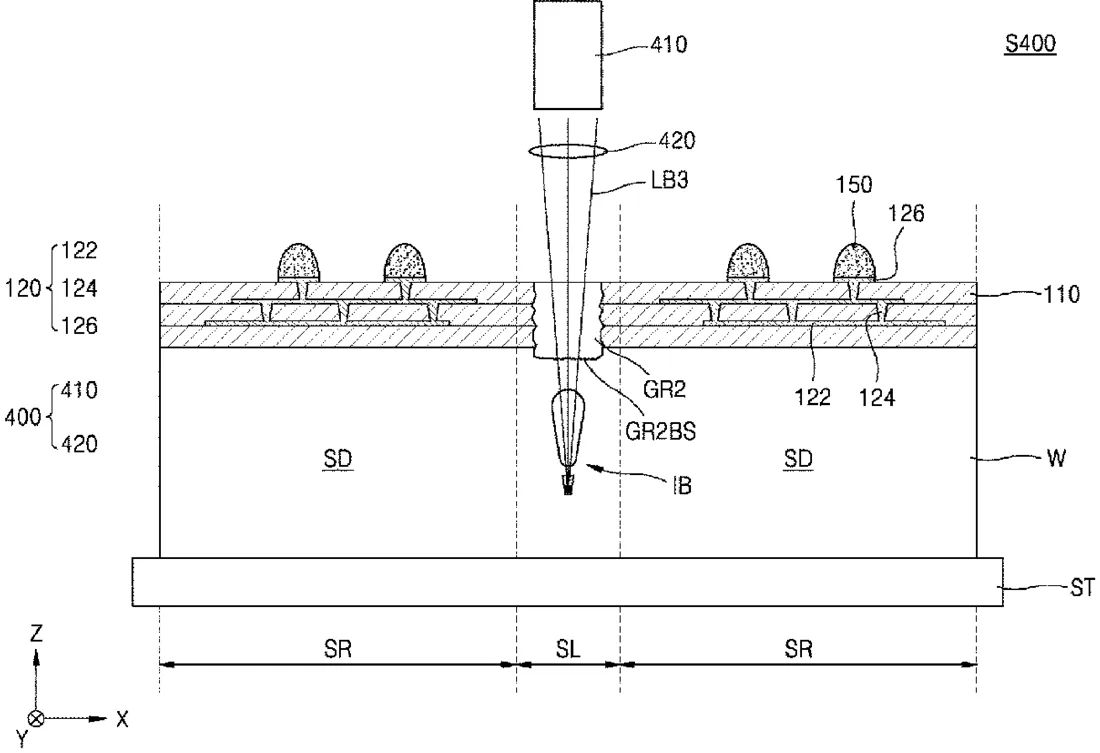
Samsung has been granted a patent for a method to cut silicon wafers into individual chips. The process uses a laser to create internal cracks along pre-cut grooves, allowing the chips to be separated cleanly without physically grinding through the entire material.
In the filing’s own words
A wafer dicing method includes preparing a wafer having a plurality of device formation areas and a scribe lane area defining the plurality of device formation areas, forming a plurality of semiconductor devices in the plurality of device formation areas of the wafer, forming, in the scribe lane area, a plurality of first grooves partially passing through at least a portion of the wafer in a vertical direction, forming a plurality of second grooves by planarizing lower surfaces of the plurality of first grooves, forming one or more internal cracks in the wafer by radiating a laser beam along lower surfaces of the plurality of second grooves, and separating the plurality of semiconductor devices from each other along the one or more internal cracks.
What exactly they claim (claim 1)
1. A wafer dicing method, comprising: preparing a wafer having a plurality of device formation areas and a scribe lane area between the plurality of device formation areas; forming a plurality of semiconductor devices in the respective plurality of device formation areas of the wafer; forming, in the scribe lane area, a plurality of first grooves partially passing through at least a portion of the wafer in a vertical direction; forming a plurality of second grooves by planarizing lower surfaces of the plurality of first grooves; forming one or more internal cracks in the wafer by radiating a laser beam along lower surfaces of the plurality of second grooves; and separating the plurality of semiconductor devices from each other along the one or more internal cracks.
Facts
- Company
- Samsung (Samsung Electronics Co., Ltd.)
- Official title
- Wafer dicing method forming internal cracks by laser beam and method of manufacturing semiconductor device by using the same
- Patent number
- US12765300B2
- Application number
- 18519501
- Filed
- Nov 27, 2023
- Granted
- Oct 13, 2026
- Inventors
- 6
- Claims
- 20
Classified under
H10P 54/30 Electricity & electronicsB23K 26/53 Operations & transportH10P 52/00 Electricity & electronicsH10P 54/00 Electricity & electronicsH10P 58/20 Electricity & electronicsH10P 72/7402 Electricity & electronicsMore from Samsung in Chips & hardware
- Samsung patents chip that combines camera and screen Oct 13, 2026
- Samsung patents faster chip testing using machine learning Sep 1, 2026
- Samsung patents radar method to pinpoint target direction more accurately Sep 1, 2026
- Samsung patents memory chip that searches data by content, not address Sep 1, 2026
- Samsung patents chip design that skips empty data to speed up AI Sep 1, 2026
Summaries are simplified from the filing’s own abstract and first claim. A patent filing is not a product announcement.
Patent data and drawings: U.S. Patent and Trademark Office (USPTO). Nebula is not affiliated with or endorsed by the USPTO.