Samsung patents stacked image sensor design with three chip layers
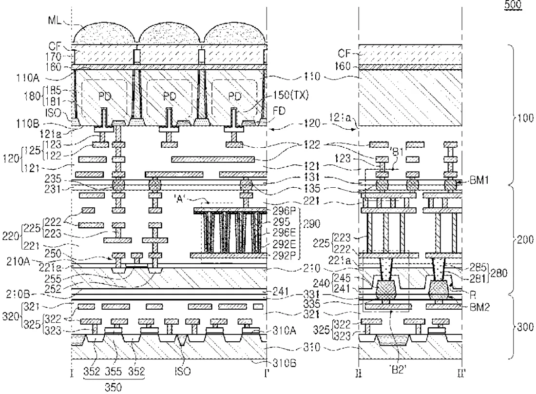
Samsung has been granted a patent for an image sensor that stacks three separate semiconductor chips vertically to create a compact camera component. The design uses specific wiring structures and bonding pads to connect the pixel layer, signal processing layer, and logic layer into a single unit.
In the filing’s own words
An image sensor is provided. The image sensor includes a first semiconductor chip including a first semiconductor substrate having a pixel unit, a first wiring structure having a first wiring layer, and a first bonding pad; a second semiconductor chip including a second semiconductor substrate having first and second surfaces, a second wiring structure on the first surface, contacting the first wiring structure, and having a second wiring layer, a second upper bonding pad bonded to the first bonding pad, and a via structure connected to the second wiring layer and extending to the second surface; a bonding layer including a bonding insulating layer on the second surface, and a second lower bonding pad connected to the via structure; and a third semiconductor chip including a third semiconductor substrate, a third wiring structure contacting the bonding insulating layer, and a third bonding pad bonded to the second lower bonding pad.
What exactly they claim (claim 1)
1. An image sensor, comprising: a first semiconductor chip including a first semiconductor substrate having a pixel unit in which a plurality of pixels are arranged, a first wiring structure on the first semiconductor substrate and having a first wiring layer, and a first bonding pad exposed to one surface of the first wiring structure and connected to the first wiring layer; a second semiconductor chip including a second semiconductor substrate having a first surface on which at least a portion of a plurality of transistors of a pixel signal generator circuit are located and a second surface opposite to the first surface, a second wiring structure on the first surface of the second semiconductor substrate, the second wiring structure having one surface in contact with the one surface of the first wiring structure, the second wiring structure having a second wiring layer, a second upper bonding pad exposed to the one surface of the second wiring structure and bonded to the first bonding pad, and a via structure connected to the second wiring layer and extending to the second surface of the second semiconductor substrate, the via structure including a via plug, and an insulating liner surrounding a side surface of the via plug, wherein the via plug includes a protruding portion that is exposed axially and protruding from the insulating liner along a longitudinal axis of the via plug; a bonding layer including a bonding insulating layer on the second surface of the second semiconductor substrate, and a second lower bonding pad buried in the bonding insulating layer and exposed to one surface of the bonding insulating layer, wherein the via plug connects the second wiring layer to the second lower bonding pad, wherein the protruding portion of the via plug contacts the second lower bonding pad, such that the second lower bonding pad is connected to the via structure; and a third semiconductor chip including a third semiconductor substrate having one surface on which logic devices are located, a third wiring structure on the one surface of the third semiconductor substrate, the third wiring structure having a third wiring layer, the third wiring structure having one surface in contact with the one surface of the bonding insulating layer, and a third bonding pad connected to the third wiring layer and exposed to the one surface of the third wiring structure, the third bonding pad bonded to the second lower bonding pad.
Facts
- Company
- Samsung (Samsung Electronics Co., Ltd.)
- Official title
- Image sensor
- Patent number
- US12765102B2
- Application number
- 18405372
- Filed
- Jan 5, 2024
- Granted
- Oct 13, 2026
- Inventors
- 4
- Claims
- 19
Classified under
H10F 39/809 Electricity & electronicsH10F 39/018 Electricity & electronicsH10F 39/811 Electricity & electronicsH10W 20/496 Electricity & electronicsH10W 80/312 Electricity & electronicsH10W 80/327 Electricity & electronicsMore from Samsung in Chips & hardware
- Samsung patents chip that combines camera and screen Oct 13, 2026
- Samsung patents faster chip testing using machine learning Sep 1, 2026
- Samsung patents radar method to pinpoint target direction more accurately Sep 1, 2026
- Samsung patents memory chip that searches data by content, not address Sep 1, 2026
- Samsung patents chip design that skips empty data to speed up AI Sep 1, 2026
Summaries are simplified from the filing’s own abstract and first claim. A patent filing is not a product announcement.
Patent data and drawings: U.S. Patent and Trademark Office (USPTO). Nebula is not affiliated with or endorsed by the USPTO.