Samsung patents method to check camera alignment during assembly
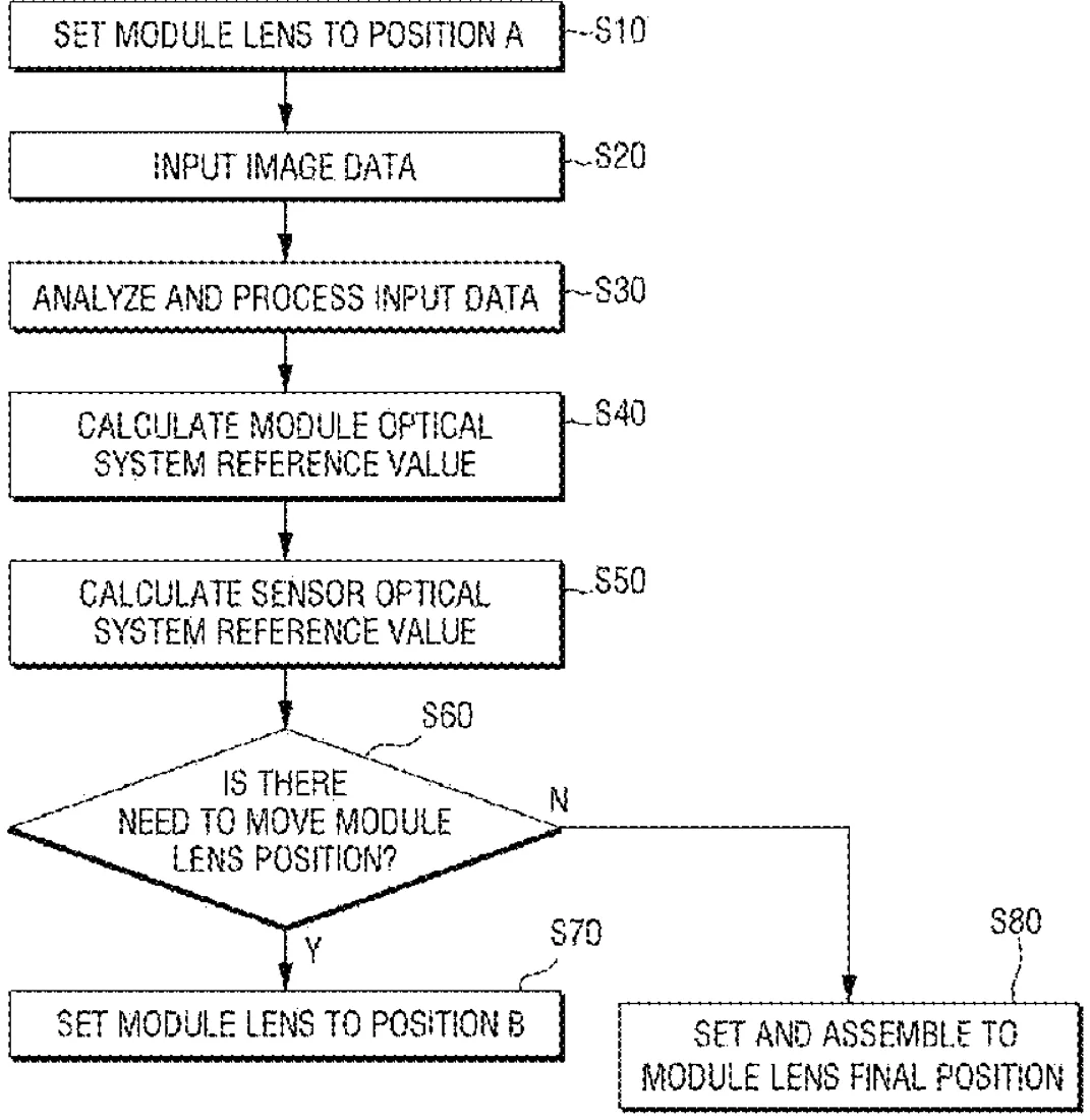
Samsung describes a way to test camera modules while they are being built. The process takes a test photo, analyzes the data to check if the lens and sensor are aligned correctly, and decides if the position needs adjusting.
In the filing’s own words
An assembly method of an image sensor module assembly device is provided. The assembly method includes: setting an image sensor and a module lens of an image sensor module at a first position; inputting image data to the image sensor module set at the first position; pre-processing data that are output from the image sensor module based on sensing the input image data; obtaining, based on the pre-processed data, a module optical system reference value of the module lens and a sensor optical system reference value of the image sensor; and determining whether to maintain the first position based on the module optical system reference value and the sensor optical system reference value.
What exactly they claim (claim 1)
1. An assembly method of an image sensor module assembly device, the method comprising: setting an image sensor and a module lens of an image sensor module at a first position; inputting image data to the image sensor module set at the first position; pre-processing data that are output from the image sensor module based on sensing the input image data; obtaining, based on the pre-processed data, a module optical system reference value of the module lens and a sensor optical system reference value of the image sensor; and determining whether to maintain the first position based on the module optical system reference value and the sensor optical system reference value, wherein the obtaining the sensor optical system reference value comprises: separating pixel values of unit pixels of the pre-processed data according to color channels; obtaining, for each color channel, a sample gain for each pixel included in a unit pixel of a corresponding color channel based on pixel values and a pixel average value of the unit pixel; and obtaining the sensor optical system reference value based on the sample gain for each pixel included in the unit pixel.
Facts
- Company
- Samsung (SAMSUNG ELECTRONICS CO., LTD.)
- Official title
- Image sensor module assembly device and assembly method for the same
- Patent number
- US12765098B2
- Application number
- 18655971
- Filed
- May 6, 2024
- Granted
- Oct 13, 2026
- Inventors
- 1
- Claims
- 20
Classified under
H10F 39/8063 Electricity & electronicsH04N 25/69 Electricity & electronicsH10F 39/802 Electricity & electronicsMore from Samsung in Chips & hardware
- Samsung patents chip that combines camera and screen Oct 13, 2026
- Samsung patents faster chip testing using machine learning Sep 1, 2026
- Samsung patents radar method to pinpoint target direction more accurately Sep 1, 2026
- Samsung patents memory chip that searches data by content, not address Sep 1, 2026
- Samsung patents chip design that skips empty data to speed up AI Sep 1, 2026
Summaries are simplified from the filing’s own abstract and first claim. A patent filing is not a product announcement.
Patent data and drawings: U.S. Patent and Trademark Office (USPTO). Nebula is not affiliated with or endorsed by the USPTO.