Samsung patents image sensor with shared charge storage for better light capture
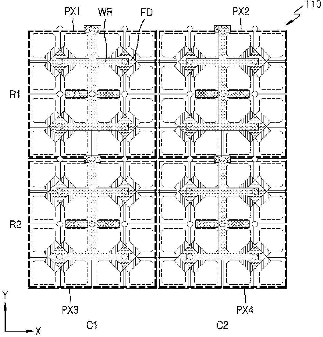
Samsung has been granted a patent for an image sensor design where four smaller light-capturing units share a common storage area for electrical charges. This setup connects these storage areas through internal wiring to manage how light data is processed within the sensor.
In the filing’s own words
A pixel array and an image sensor including the pixel array are provided. The pixel array included in the image sensor includes a plurality of pixels arranged in a matrix, and a plurality of column lines each commonly connected to pixels arranged on a same column from among the plurality of pixels. Each of the plurality of pixels includes four subpixels. Each of the four subpixels includes four photoelectric conversion devices; a floating diffusion region storing electric charges generated by the four photoelectric conversion devices; and four transmission gates configured to transmit the electric charges generated by the four photoelectric conversion devices to the floating diffusion region. Four floating diffusion regions included in the four subpixels are electrically connected to one another via internal wiring. Each of the plurality of pixels further includes a reset gate, a first driving gate and a first selection gate.
What exactly they claim (claim 1)
1. An image sensor comprising: a substrate comprising a first surface and a second surface opposite the first surface; a first pixel comprising first-four photoelectric conversion devices (PDs) and a first floating diffusion (FD) region shared by the first-four PDs in the substrate; a second pixel comprising second-four PDs and a second FD region shared by the second-four PDs in the substrate; a third pixel comprising third-four PDs and a third FD region shared by the third-four PDs in the substrate; a fourth pixel comprising fourth-four PDs and a fourth FD region shared by the fourth-four PDs in the substrate; a reset transistor configured to connect to a pixel power supply voltage; and a gain control transistor configured to connect to the reset transistor, wherein the first FD region is connected to the fourth FD region through a first wiring, wherein the second FD region is connected to the third FD region through a second wiring, wherein each of the first-four PDs to the fourth-four PDs are arranged in a 2×2 matrix, and wherein the reset transistor is configured to provide the pixel power supply voltage to the first to fourth FD regions.
Facts
- Company
- Samsung (Samsung Electronics Co., Ltd.)
- Official title
- Pixel array and image sensor including the same
- Patent number
- US12765086B2
- Application number
- 19060920
- Filed
- Feb 24, 2025
- Granted
- Oct 13, 2026
- Inventors
- 2
- Claims
- 19
Classified under
H10F 39/802 Electricity & electronicsH04N 25/75 Electricity & electronicsH04N 25/772 Electricity & electronicsH04N 25/78 Electricity & electronicsH10F 39/8053 Electricity & electronicsH10F 39/8063 Electricity & electronicsMore from Samsung in Chips & hardware
- Samsung patents chip that combines camera and screen Oct 13, 2026
- Samsung patents faster chip testing using machine learning Sep 1, 2026
- Samsung patents radar method to pinpoint target direction more accurately Sep 1, 2026
- Samsung patents memory chip that searches data by content, not address Sep 1, 2026
- Samsung patents chip design that skips empty data to speed up AI Sep 1, 2026
Summaries are simplified from the filing’s own abstract and first claim. A patent filing is not a product announcement.
Patent data and drawings: U.S. Patent and Trademark Office (USPTO). Nebula is not affiliated with or endorsed by the USPTO.