Samsung patents chip design with thicker side walls to protect transistors
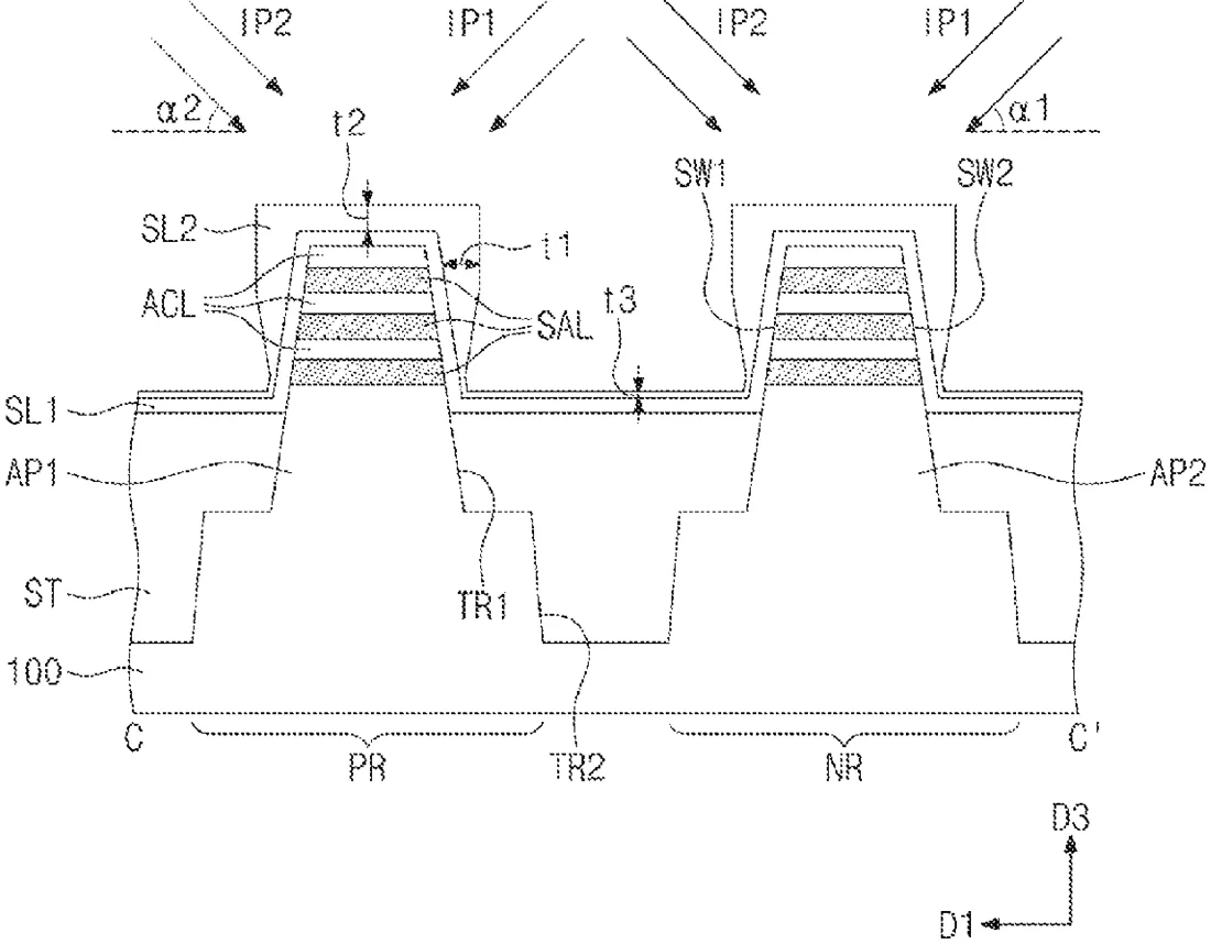
Samsung has secured a patent for a method to build semiconductor chips that uses specific spacing layers around the transistor parts. The design features a thicker protective layer on the side of the source and drain areas compared to the gate area. This structure is created during the manufacturing process by depositing material in specific directions before removing the temporary guide structures.
In the filing’s own words
A semiconductor device is disclosed. The semiconductor device may include an active pattern on a substrate, source/drain patterns on the active pattern, a fence spacer on side surfaces of each of the source/drain patterns, a channel pattern interposed between the source/drain patterns, a gate electrode crossing the channel pattern and extending in a first direction, and a gate spacer on a side surface of the gate electrode. A first thickness of an upper portion of the fence spacer in the first direction may be greater than a second thickness of the gate spacer in a second direction crossing the first direction.
What exactly they claim (claim 1)
1. A method of fabricating a semiconductor device, comprising: forming active patterns extending in a second direction on a substrate; forming sacrificial gate patterns crossing the active patterns and extending in a first direction; forming a first spacer layer on side surfaces of the active patterns and side surfaces of the sacrificial gate patterns; performing a first directional deposition process on the first spacer layer in the first direction and in a direction opposite to the first direction to form a second spacer layer on the first spacer layer; removing portions of the active patterns that are exposed between the sacrificial gate patterns to form recesses between the sacrificial gate patterns; forming source/drain patterns in the recesses; and replacing the sacrificial gate patterns with gate electrodes.
Facts
- Company
- Samsung (Samsung Electronics Co., Ltd.)
- Official title
- Semiconductor device and method of fabricating the same
- Patent number
- US12765052B2
- Application number
- 18430902
- Filed
- Feb 2, 2024
- Granted
- Oct 13, 2026
- Inventors
- 4
- Claims
- 20
Classified under
H10D 84/856 Electricity & electronicsMore from Samsung in Chips & hardware
- Samsung patents chip that combines camera and screen Oct 13, 2026
- Samsung patents faster chip testing using machine learning Sep 1, 2026
- Samsung patents radar method to pinpoint target direction more accurately Sep 1, 2026
- Samsung patents memory chip that searches data by content, not address Sep 1, 2026
- Samsung patents chip design that skips empty data to speed up AI Sep 1, 2026
Summaries are simplified from the filing’s own abstract and first claim. A patent filing is not a product announcement.
Patent data and drawings: U.S. Patent and Trademark Office (USPTO). Nebula is not affiliated with or endorsed by the USPTO.