Samsung patents chip method to fix timing errors in data transfer
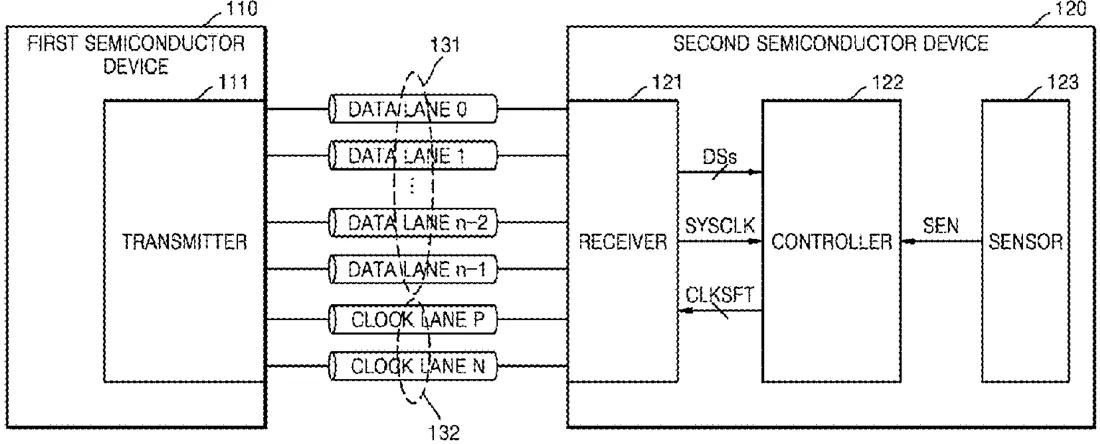
This patent describes a semiconductor device that uses a special 'track signal' to check if internal clock signals are perfectly aligned. A controller compares how often the track signal is read by two different clock phases to detect any timing drift, or skew. It then sends a correction signal to shift the clock phases, ensuring data is read accurately.
In the filing’s own words
A semiconductor device includes a receiver and a controller. The receiver is configured to sample a data signal and a track signal received through data lanes in response to rising edges of first and second internal clock signal pairs. The controller is configured to detect a skew status between the track signal and the first and second internal clock signal pairs, based on the number of times a specific logic level of the track signal is sampled in synchronization with each of the first and second internal clock signal pairs, and provide the receiver with a clock shift signal for calibrating a clock skew, based on the skew status.
What exactly they claim (claim 1)
1. A semiconductor device comprising: a receiver configured to: receive a data signal through a first data lane, receive a track signal through a second data lane, receive an external clock signal pair through a complementary clock lane, generate first and second internal clock signal pairs of different phases, based on the external clock signal pair, to sample the data signal and the track signal in response to edges of the first and second internal clock signal pairs, and output digital signals comprising logic levels of the sampled data signal and the sampled track signal; and a controller configured to: receive the digital signals, detect a skew status between the track signal and the first and second internal clock signal pairs, based on a first number of times a specific logic level of the track signal is sampled in synchronization with the first internal clock signal pair and a second number of times the specific logic level of the track signal is sampled in synchronization with the second internal clock signal pair, and provide a clock shift signal comprising a shift magnitude and a shift direction to shift phases of the first and second internal clock signal pairs, based on the skew status.
Facts
- Company
- Samsung (SAMSUNG ELECTRONICS CO., LTD.)
- Official title
- Semiconductor package calibrating skew of clock signal, semiconductor device, and operating method of the semiconductor device
- Patent number
- US12763779B2
- Application number
- 19007266
- Filed
- Dec 31, 2024
- Granted
- Oct 13, 2026
- Inventors
- 7
- Claims
- 20
Classified under
H03L 7/0814 Electricity & electronicsH03K 3/037 Electricity & electronicsH03L 7/091 Electricity & electronicsMore from Samsung in Chips & hardware
- Samsung patents chip that combines camera and screen Oct 13, 2026
- Samsung patents faster chip testing using machine learning Sep 1, 2026
- Samsung patents radar method to pinpoint target direction more accurately Sep 1, 2026
- Samsung patents memory chip that searches data by content, not address Sep 1, 2026
- Samsung patents chip design that skips empty data to speed up AI Sep 1, 2026
Summaries are simplified from the filing’s own abstract and first claim. A patent filing is not a product announcement.
Patent data and drawings: U.S. Patent and Trademark Office (USPTO). Nebula is not affiliated with or endorsed by the USPTO.