Samsung patents NAND memory that repairs itself during rewrites
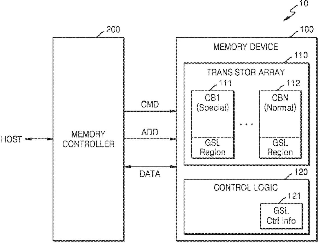
This filing describes a method for managing NAND flash memory, the type used in SSDs and phones, by using two separate groups of control transistors. The system checks if these transistors are wearing out and performs a specific erase step on the first group before testing the second group to ensure the memory remains stable.
In the filing’s own words
A memory device is provided. The memory device includes: memory cells respectively connected with word lines; first ground selection transistors connected with a first ground selection line programmed to have a first threshold voltage; second ground selection transistors connected with a second ground selection line programmed to have a second threshold voltage which differs from the first threshold voltage; and a control circuit configured to: control an erase operation to be performed on each of at least one first ground selection transistor of the first ground selection transistors based on a threshold voltage of each of the at least one first ground selection transistor being greater than a predetermined first criterion; and control a threshold voltage of each of the second ground selection transistors to be compared with a predetermined second criterion based on the erase operation on the at least one first ground selection transistor being completed.
What exactly they claim (claim 1)
1. A memory device comprising: a plurality of memory cells respectively connected with a plurality of word lines; a plurality of first ground selection transistors connected with a first ground selection line that is programmed to have a first threshold voltage; a plurality of second ground selection transistors connected with a second ground selection line that is programmed to have a second threshold voltage which differs from the first threshold voltage; and a control circuit configured to: control an erase operation to be performed on each of at least one first ground selection transistor of the plurality of first ground selection transistors based on a threshold voltage of each of the at least one first ground selection transistor being greater than a predetermined first criterion; and control a threshold voltage of each of the plurality of second ground selection transistors to be compared with a predetermined second criterion based on the erase operation on the at least one first ground selection transistor being completed.
Facts
- Company
- Samsung (SAMSUNG ELECTRONICS CO., LTD.)
- Official title
- Nand flash memory device with a rewrite operation and operating method thereof
- Patent number
- US12763146B2
- Application number
- 18537344
- Filed
- Dec 12, 2023
- Granted
- Oct 13, 2026
- Inventors
- 2
- Claims
- 20
Classified under
G11C 16/102 Physics & computingG11C 16/0433 Physics & computingG11C 16/16 Physics & computingG11C 16/08 Physics & computingMore from Samsung in Chips & hardware
- Samsung patents chip that combines camera and screen Oct 13, 2026
- Samsung patents faster chip testing using machine learning Sep 1, 2026
- Samsung patents radar method to pinpoint target direction more accurately Sep 1, 2026
- Samsung patents memory chip that searches data by content, not address Sep 1, 2026
- Samsung patents chip design that skips empty data to speed up AI Sep 1, 2026
Summaries are simplified from the filing’s own abstract and first claim. A patent filing is not a product announcement.
Patent data and drawings: U.S. Patent and Trademark Office (USPTO). Nebula is not affiliated with or endorsed by the USPTO.