Samsung patents memory circuit that self-adjusts data reading timing
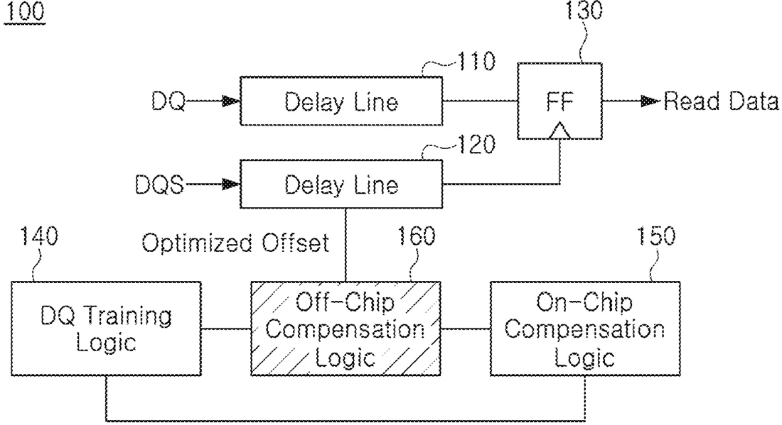
Samsung has been granted a patent for a circuit inside storage devices like SSDs that improves how data is read from nonvolatile memory. The system uses multiple timing paths to sample data signals and compares them to find the most reliable reading window. It then adjusts the timing offsets to compensate for variations in the hardware, ensuring accurate data retrieval.
In the filing’s own words
A storage device includes at least one nonvolatile memory device, and a controller configured to control the at least one nonvolatile memory device, wherein the controller includes a nonvolatile memory interface circuit configured to communicate with the at least one nonvolatile memory device through at least one channel, wherein the nonvolatile memory interface circuit includes a margin collector configured to collect margin information by comparing read data with sampling data, an on-chip margin search logic configured to track a valid window margin by adjusting an offset value based on the margin information, and a compensation calculator configured to determine off-chip variation corresponding to the offset value when the valid window margin is in a margin lock state.
What exactly they claim (claim 1)
1. A nonvolatile memory interface circuit comprising: a main path circuit configured to capture a data signal using a data strobe signal delayed based on offset information, and to output read data based on the data signal; a first capture path circuit configured to generate a plurality of first sampling data strobe signals by delaying the data strobe signal using first offset information, and to capture the data signal in response to each first sampling data strobe signal of the plurality of first sampling data strobe signals to output first sampling data; a second capture path circuit configured to generate a plurality of second sampling data strobe signals by delaying the data strobe signal using second offset information, and to capture the data signal in response to each second sampling data strobe signal of the plurality of second sampling data strobe signals to output second sampling data; and an off-chip compensation logic configured to determine a first error count between the read data and the first sampling data, and determine a second error count between the read data and the second sampling data, and to correct the offset information, the first offset information, and the second offset information using the first error count and the second error count.
Facts
- Company
- Samsung (SAMSUNG ELECTRONICS CO., LTD.)
- Official title
- Nonvolatile memory interface circuit, storage device having the same and method of operating the same
- Patent number
- US12763118B2
- Application number
- 18758015
- Filed
- Jun 28, 2024
- Granted
- Oct 13, 2026
- Inventors
- 1
- Claims
- 20
Classified under
G11C 7/222 Physics & computingG06F 3/061 Physics & computingG06F 3/0655 Physics & computingG06F 3/0679 Physics & computingG11C 7/1069 Physics & computingG11C 7/1096 Physics & computingMore from Samsung in Chips & hardware
- Samsung patents chip that combines camera and screen Oct 13, 2026
- Samsung patents faster chip testing using machine learning Sep 1, 2026
- Samsung patents radar method to pinpoint target direction more accurately Sep 1, 2026
- Samsung patents memory chip that searches data by content, not address Sep 1, 2026
- Samsung patents chip design that skips empty data to speed up AI Sep 1, 2026
Summaries are simplified from the filing’s own abstract and first claim. A patent filing is not a product announcement.
Patent data and drawings: U.S. Patent and Trademark Office (USPTO). Nebula is not affiliated with or endorsed by the USPTO.