Samsung patents memory chip circuit that self-adjusts signal strength
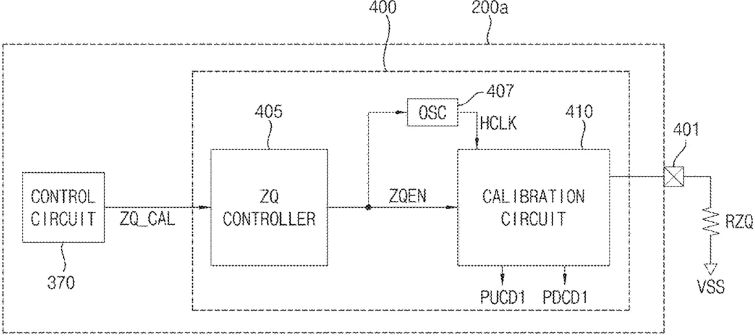
This patent describes a circuit inside semiconductor memory that automatically adjusts how strongly it pushes or pulls electrical signals. It compares internal voltages to external resistors on the circuit board to ensure data transfers remain stable and accurate.
In the filing’s own words
An impedance calibration circuit includes a calibration controller and a calibration circuit. The calibration controller generates a calibration enable signal based on an impedance calibration command. The calibration circuit, connected to an external resistor through an impedance pad, generates, in response to the calibration enable signal, a first reference voltage code when a voltage level of a selected reference voltage becomes the same as a first voltage of a first node, coupled to the impedance pad. The calibration circuit generates a pull-up control code based on the first reference voltage code, generates a second reference voltage code when the voltage level of the selected reference voltage becomes the same as a second voltage of a second node, and generates a pull-down control code based on the second reference voltage code.
What exactly they claim (claim 1)
1. An impedance calibration circuit, comprising: a calibration controller configured to receive an impedance calibration command and generate a calibration enable signal based on the impedance calibration command; an oscillator configured to generate a clock signal in response to the calibration enable signal; and a calibration circuit connected to an external resistor provided in a board through an impedance pad, the calibration circuit being configured to, in response to the calibration enable signal: generate a first reference voltage code based on a voltage level of a selected reference voltage becoming the same as a first voltage of a first node coupled to the impedance pad, the first voltage being based on an initial pull-up control code; generate a pull-up control code for driving the first node based on the first reference voltage code; generate a second reference voltage code based on the voltage level of the selected reference voltage becoming the same as a second voltage of a second node, the second voltage being based on the pull-up control code; and generate a pull-down control code for driving the second node based on the second reference voltage code, wherein the calibration circuit includes a pull-up driver coupled between a power supply voltage and the first node, the pull-up driver configured to drive the first node with the first voltage based on the initial pull-up control code, a first comparator circuit configured to generate a first comparison signal by comparing the first voltage with the selected reference voltage, a reference voltage generator configured to generate a plurality of reference voltages, a replica pull-up driver coupled between the power supply voltage and the second node, the replica pull-up driver configured to drive the second node with the second voltage based on the pull-up control code, a pull-down driver coupled between the second node and a ground voltage, a second comparator circuit configured to generate a second comparison signal by comparing the second voltage with the selected reference voltage, and a control/code generation circuit configured to select the selected reference voltage from among the plurality of reference voltages, generate the first reference voltage code based on the first comparison signal, generate the pull-up control code based on the first reference voltage code, generate the second reference voltage code based on the second comparison signal, generate the pull-down control code based on the second reference voltage code, and provide the pull-down control code to the pull-down driver, wherein the control/code generation circuit includes a selection signal generator configured to generate selection signals and inverted selection signals based on the clock signal, and a reference voltage selector configured to output the selected reference voltage by selecting at least a portion of the plurality of reference voltages based on the selection signals and the inverted selection signals during each of a plurality of cycles.
Facts
- Company
- Samsung (Samsung Electronics Co., Ltd.)
- Official title
- Impedance calibration circuits and semiconductor memory devices including the same
- Patent number
- US12763117B2
- Application number
- 18936744
- Filed
- Nov 4, 2024
- Granted
- Oct 13, 2026
- Inventors
- 5
- Claims
- 18
Classified under
G11C 7/1048 Physics & computingH03K 19/0005 Electricity & electronicsG11C 2207/2254 Physics & computingMore from Samsung in Chips & hardware
- Samsung patents chip that combines camera and screen Oct 13, 2026
- Samsung patents faster chip testing using machine learning Sep 1, 2026
- Samsung patents radar method to pinpoint target direction more accurately Sep 1, 2026
- Samsung patents memory chip that searches data by content, not address Sep 1, 2026
- Samsung patents chip design that skips empty data to speed up AI Sep 1, 2026
Summaries are simplified from the filing’s own abstract and first claim. A patent filing is not a product announcement.
Patent data and drawings: U.S. Patent and Trademark Office (USPTO). Nebula is not affiliated with or endorsed by the USPTO.