Samsung patents stacked memory design to save space in chips
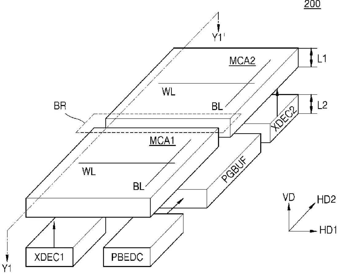
Samsung has secured a patent for a non-volatile memory device that stacks two layers of semiconductor material vertically. The design places the circuitry that reads and writes data directly above the boundary where two separate memory cell arrays meet, allowing the components to share space more efficiently.
In the filing’s own words
A non-volatile memory device includes a first semiconductor layer including a first cell region in which a first memory cell array is disposed, a second cell region in which a second memory cell array is disposed, wherein the first memory cell array and the second memory cell array each include a plurality of word lines, a plurality of memory cells, and a plurality of bit lines, and a second semiconductor layer including a page buffer circuit region in which a page buffer circuit connected to the first memory cell array and the second memory cell array is disposed, wherein the page buffer circuit region overlaps a boundary region between the first cell region and the second cell region when viewed from the vertical direction.
What exactly they claim (claim 1)
1. A non-volatile memory device comprising: a first semiconductor layer comprising a first cell region in which a first memory cell array is disposed, a second cell region in which a second memory cell array is disposed, and a first metal pad layer, wherein the first memory cell array and the second memory cell array each comprise a plurality of word lines stacked in a vertical direction, a plurality of memory cells respectively connected to the plurality of word lines, and a plurality of bit lines; and a second semiconductor layer comprising a page buffer circuit region in which a page buffer circuit connected to the first memory cell array and the second memory cell array is disposed, and a second metal pad layer, wherein the second semiconductor layer is connected to the first semiconductor layer in the vertical direction through bonding by the first metal pad layer and the second metal pad layer, wherein the page buffer circuit includes at least one transistor that overlaps a boundary region within the first semiconductor layer between the first cell region and the second cell region when viewed from the vertical direction, wherein the page buffer circuit comprises, within the second semiconductor layer: a first switch connected between a page buffer and a first bit line connected to the first memory cell array; a second switch connected between the page buffer and a second bit line connected to the second memory cell array; and the page buffer comprising a sensing latch connected to the first switch and the second switch in common, and wherein at least one of the first switch, the second switch, and the page buffer overlaps the boundary region when viewed from the vertical direction.
Facts
- Company
- Samsung (Samsung Electronics Co., Ltd.)
- Official title
- Non-volatile memory device
- Patent number
- US12763116B2
- Application number
- 18104533
- Filed
- Feb 1, 2023
- Granted
- Oct 13, 2026
- Inventors
- 2
- Claims
- 20
Classified under
G11C 7/1039 Physics & computingG11C 5/063 Physics & computingG11C 7/1069 Physics & computingMore from Samsung in Chips & hardware
- Samsung patents chip that combines camera and screen Oct 13, 2026
- Samsung patents faster chip testing using machine learning Sep 1, 2026
- Samsung patents radar method to pinpoint target direction more accurately Sep 1, 2026
- Samsung patents memory chip that searches data by content, not address Sep 1, 2026
- Samsung patents chip design that skips empty data to speed up AI Sep 1, 2026
Summaries are simplified from the filing’s own abstract and first claim. A patent filing is not a product announcement.
Patent data and drawings: U.S. Patent and Trademark Office (USPTO). Nebula is not affiliated with or endorsed by the USPTO.