Samsung patents display circuit that uses dummy channels to stabilize voltage
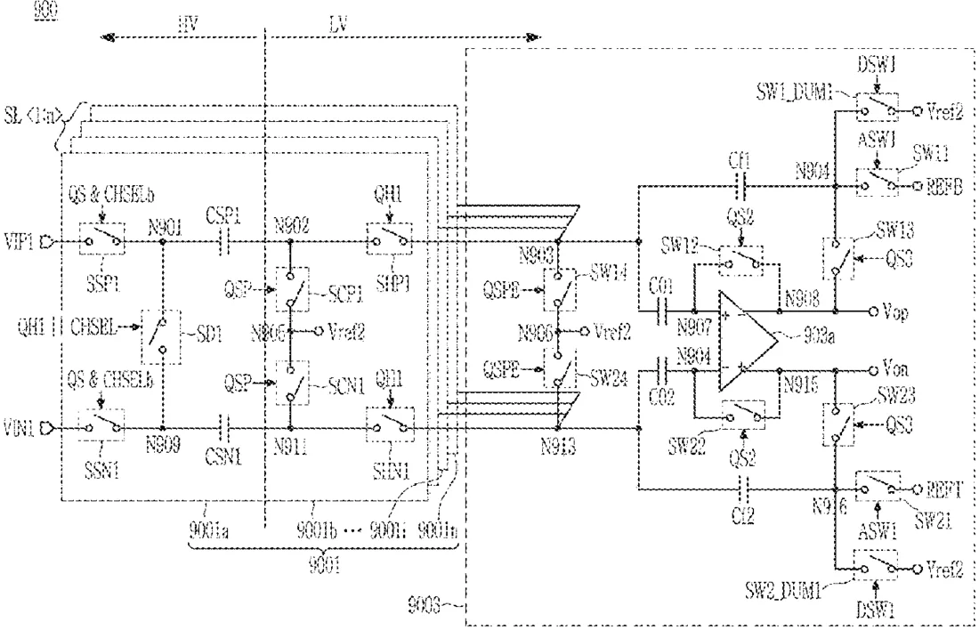
This filing describes a display device that includes extra 'dummy' channels alongside the visible pixels. It uses specific circuits to sample voltages from these dummy channels and amplify them to help manage the power signals sent to the screen.
In the filing’s own words
A display device including a plurality of channels including at least one dummy channel; a plurality of first sampling circuits sampling a plurality of dummy voltages corresponding to each of the at least one dummy channel; and a holding/scaling circuit including a first input node, a second input node, a first output node, a second output node, a first feedback capacitor connected between the first input node and the first output node, and a second feedback capacitor connected between the second input node and the second output node.
What exactly they claim (claim 1)
1. A display device comprising: a plurality of channels, the plurality of channels include at least one dummy channel; a plurality of first sampling circuits, each configured to sample one of a plurality of dummy voltages corresponding to each of the at least one dummy channel, each dummy voltage of the plurality of dummy voltages comprises a respective floating dummy voltage different from a pixel voltage; and a holding/scaling circuit including a first input node, a second input node, a first output node, a second output node, a first feedback capacitor connected between the first input node and the first output node, and a second feedback capacitor connected between the second input node and the second output node, wherein the holding/scaling circuit is configured to: store voltages of substantially a same magnitude in the first feedback capacitor and the second feedback capacitor, receive the plurality of sampled dummy voltages from the first input node and the second input node, and output a plurality of dummy output voltages acquired by amplifying the plurality of sampled dummy voltages to the first output node and the second output node.
Facts
- Company
- Samsung (SAMSUNG ELECTRONICS CO., LTD.)
- Official title
- Display device and method of driving the same
- Patent number
- US12762980B2
- Application number
- 18779983
- Filed
- Jul 22, 2024
- Granted
- Oct 13, 2026
- Inventors
- 4
- Claims
- 20
Classified under
G09G 3/006 Physics & computingG09G 3/2096 Physics & computingG09G 3/3233 Physics & computingG09G 3/3275 Physics & computingG09G 2300/0819 Physics & computingG09G 2300/0842 Physics & computingMore from Samsung in Chips & hardware
- Samsung patents chip that combines camera and screen Oct 13, 2026
- Samsung patents faster chip testing using machine learning Sep 1, 2026
- Samsung patents radar method to pinpoint target direction more accurately Sep 1, 2026
- Samsung patents memory chip that searches data by content, not address Sep 1, 2026
- Samsung patents chip design that skips empty data to speed up AI Sep 1, 2026
Summaries are simplified from the filing’s own abstract and first claim. A patent filing is not a product announcement.
Patent data and drawings: U.S. Patent and Trademark Office (USPTO). Nebula is not affiliated with or endorsed by the USPTO.