Samsung patents memory chip design using multi-phase signal conversion
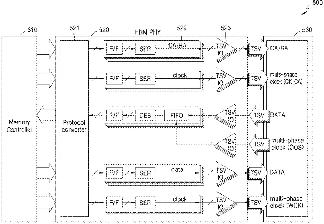
Samsung describes a semiconductor device where a logic die controls a memory core die through vertical connections called through-silicon vias. The logic die includes a protocol converter that changes how data signals are sent to support multi-phase communication, allowing for synchronized data processing.
In the filing’s own words
A semiconductor device includes at least one core die and a logic die communicating with the core die via a plurality of through-silicon vias. The logic die includes a memory controller configured to control a memory operation of the core die and a PHY region configured to receive first input signals based on a first protocol from the memory controller and transmit first output signals generated based on the first input signals to the core die via the plurality of TSVs. The PHY region includes a protocol converter configured to perform alignment processing on bits of the first input signals so as to convert the protocol of the first input signals into a second protocol and then output the first input signals based on the second protocol, wherein the second protocol supports multi-phase communication between the PHY region and the core die.
What exactly they claim (claim 1)
1. A semiconductor device comprising: at least one core die comprising a memory cell array; and a logic die communicating with the at least one core die via a plurality of through-silicon vias (TSVs), wherein the logic die comprises: a memory controller configured to control a memory operation of the at least one core die; and a physical (PHY) region configured to receive first input signals based on a first protocol from the memory controller, generate first output signals of a second protocol based on the first input signals, and transmit the first output signals to the at least one core die via the plurality of TSVs, wherein the PHY region comprises: a protocol converter configured to perform alignment processing on first bits of the first input signals so as to convert the first input signals from the first protocol into the first output signals of the second protocol; and a plurality of signal processing blocks configured to process the first output signals in parallel and in synchronization with respective phases of a plurality of internal clocks having multi-phases, and wherein the second protocol is based on a multi-phase communication between the PHY region and the at least one core die.
Facts
- Company
- Samsung (SAMSUNG ELECTRONICS CO., LTD.)
- Official title
- Memory controller communicating with vertically stacked dies and semiconductor device including the same
- Patent number
- US12762078B2
- Application number
- 18979918
- Filed
- Dec 13, 2024
- Granted
- Oct 13, 2026
- Inventors
- 7
- Claims
- 20
Classified under
G06F 13/387 Physics & computingG06F 13/1689 Physics & computingMore from Samsung in Chips & hardware
- Samsung patents chip that combines camera and screen Oct 13, 2026
- Samsung patents faster chip testing using machine learning Sep 1, 2026
- Samsung patents radar method to pinpoint target direction more accurately Sep 1, 2026
- Samsung patents memory chip that searches data by content, not address Sep 1, 2026
- Samsung patents chip design that skips empty data to speed up AI Sep 1, 2026
Summaries are simplified from the filing’s own abstract and first claim. A patent filing is not a product announcement.
Patent data and drawings: U.S. Patent and Trademark Office (USPTO). Nebula is not affiliated with or endorsed by the USPTO.