Samsung patents laser method to fix tiny errors in chip masks
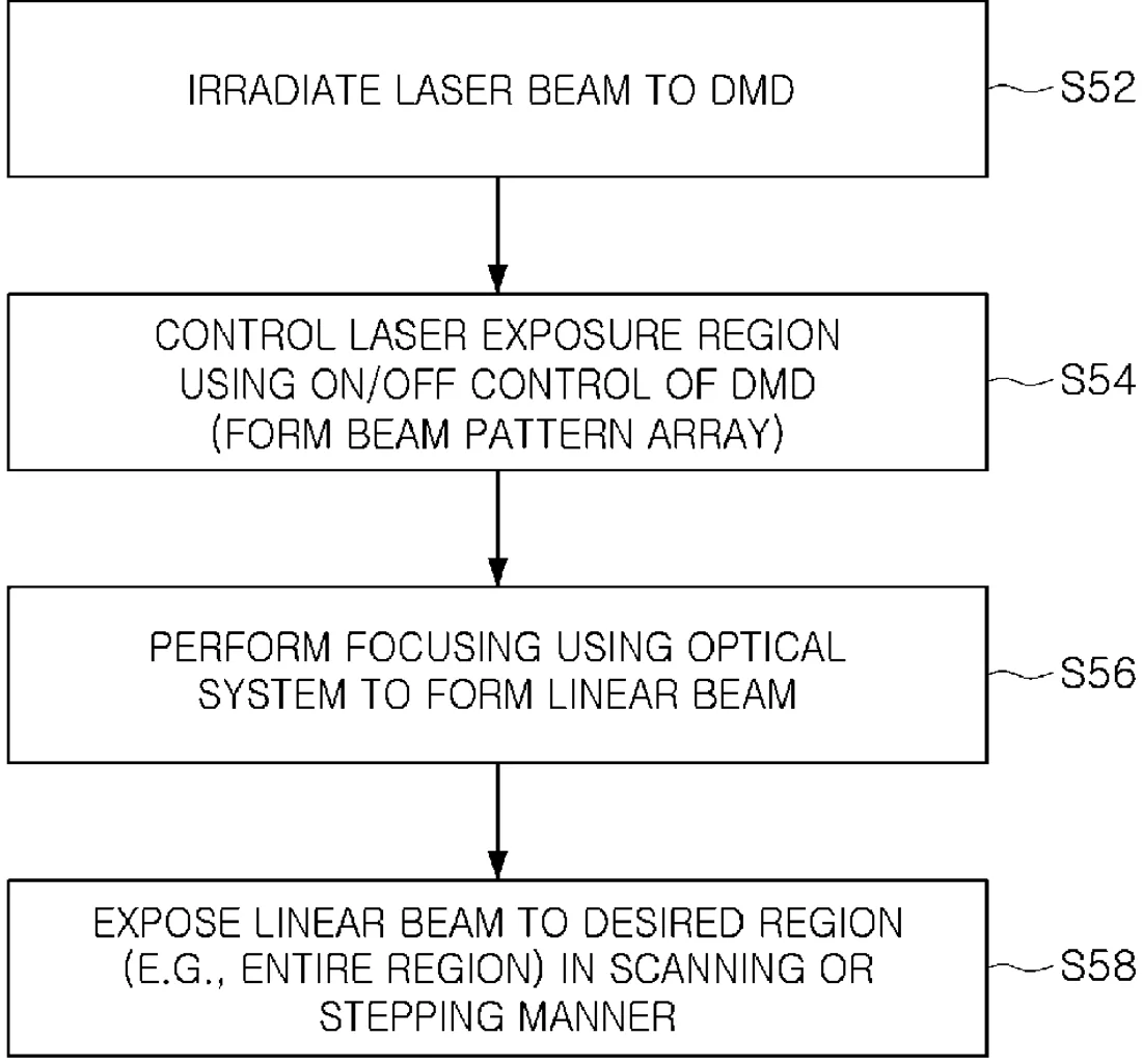
Samsung has patented a method for manufacturing photomasks, which are the stencils used to print circuits onto computer chips. The process uses a digital micromirror device to shape a laser beam into a specific line pattern, which is then used to etch away material and correct tiny size deviations in the mask's design.
In the filing’s own words
A method of manufacturing a photomask includes forming a photomask having a plurality of pattern elements, wherein the plurality of pattern elements include correction-target pattern elements having a critical dimension (CD) deviation; acquiring local CD correction information; directing a laser beam to a mirror array of a digital micromirror device (DMD), wherein the mirror array has mirrors arranged in a plurality of rows and a plurality of columns; converting the laser beam into a beam pattern array corresponding to the mirror array by controlling on/off switching of each of the mirrors based on the local CD correction information; forming a linear beam by focusing the beam pattern array through an optical system; applying an etchant to the photomask and directing the linear beam to the photomask and moving the linear beam to irradiate the photomask.
What exactly they claim (claim 1)
1. A method of manufacturing a photomask, the method comprising: forming a photomask comprising a plurality of pattern elements, wherein the plurality of pattern elements comprise correction-target pattern elements having a critical dimension (CD) deviation from a target CD; acquiring local CD correction information including position and the CD deviation of the correction-target pattern elements in the photomask; directing a laser beam to a mirror array of a digital micromirror device (DMD), wherein the mirror array has mirrors arranged in a plurality of rows and a plurality of columns; converting the laser beam into a beam pattern array corresponding to the mirror array by controlling on/off switching of each of the mirrors based on the local CD correction information, wherein the beam pattern array has a beam pattern arranged in a position corresponding to on-state mirrors in the mirror array; forming a linear beam by focusing the beam pattern array through an optical system; and performing CD correction of an area of the photomask, the CD correction comprising applying an etchant to the photomask, directing the linear beam to the photomask, and moving the linear beam to irradiate the area.
Facts
- Company
- Samsung (SAMSUNG ELECTRONICS CO., LTD.)
- Official title
- Method of manufacturing photomask, and method of manufacturing semiconductor device using the same
- Patent number
- US12761548B2
- Application number
- 18328395
- Filed
- Jun 2, 2023
- Granted
- Oct 13, 2026
- Inventors
- 4
- Claims
- 20
Classified under
G03F 1/74 Physics & computingG03F 1/24 Physics & computingH10P 76/2041 Electricity & electronicsMore from Samsung in Chips & hardware
- Samsung patents chip that combines camera and screen Oct 13, 2026
- Samsung patents faster chip testing using machine learning Sep 1, 2026
- Samsung patents radar method to pinpoint target direction more accurately Sep 1, 2026
- Samsung patents memory chip that searches data by content, not address Sep 1, 2026
- Samsung patents chip design that skips empty data to speed up AI Sep 1, 2026
Summaries are simplified from the filing’s own abstract and first claim. A patent filing is not a product announcement.
Patent data and drawings: U.S. Patent and Trademark Office (USPTO). Nebula is not affiliated with or endorsed by the USPTO.