Samsung patents nanocrystals for brighter, more stable display screens
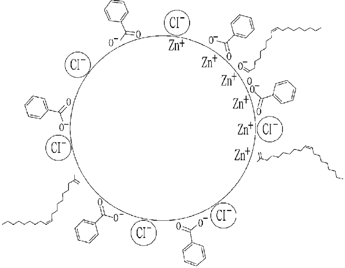
Samsung has secured a patent for a specific type of semiconductor nanocrystal used in display technology. The invention describes a core-shell structure where the surface is coated with specific organic molecules and inorganic salts to improve stability and light emission.
In the filing’s own words
A semiconductor nanocrystal including an anion of an inorganic metal salt and a first organic ligand bound to a surface of the semiconductor nanocrystal, wherein the first organic ligand includes a substituted or unsubstituted C6 to C30 aromatic ring group and a carboxylate, a substituted or unsubstituted C3 to C30 aromatic hetero cyclic group and a carboxylate, or a combination thereof.
What exactly they claim (claim 1)
1. A semiconductor nanocrystal comprising an anion of an inorganic metal salt bound to a surface of the semiconductor nanocrystal, wherein the inorganic metal salt comprises an inorganic metal halide, an inorganic metal sulfate, an inorganic metal nitrate, an inorganic metal thiocyanate, or a combination thereof, a first organic ligand bound to the surface of the semiconductor nanocrystal, wherein the first organic ligand comprises a substituted or unsubstituted C6 to C30 aromatic ring group and a carboxylate group, a substituted or unsubstituted C3 to C30 aromatic heterocyclic group and a carboxylate group, or a combination thereof, and a second organic ligand, wherein the semiconductor nanocrystal comprises a core comprising a first semiconductor nanocrystal and a shell disposed on the core, the shell comprising a second semiconductor nanocrystal having a composition different than that of the first semiconductor nanocrystal, and wherein a weight ratio of the second organic ligand, the anion of the inorganic metal salt, and the first organic ligand is about 30 to 60:30 to 60:10 to 30, respectively.
Facts
- Company
- Samsung (SAMSUNG ELECTRONICS CO., LTD.)
- Official title
- Semiconductor nanocrystal, light-emitting film, production method of the light-emitting film, light emitting device, and display device
- Patent number
- US12760222B2
- Application number
- 18535107
- Filed
- Dec 11, 2023
- Granted
- Oct 13, 2026
- Inventors
- 7
- Claims
- 16
Classified under
C09K 11/703 Chemistry & metalsC09K 11/883 Chemistry & metalsB82Y 20/00 Operations & transportB82Y 30/00 Operations & transportB82Y 40/00 Operations & transportH10K 50/115 Electricity & electronicsMore from Samsung in Chips & hardware
- Samsung patents chip that combines camera and screen Oct 13, 2026
- Samsung patents faster chip testing using machine learning Sep 1, 2026
- Samsung patents radar method to pinpoint target direction more accurately Sep 1, 2026
- Samsung patents memory chip that searches data by content, not address Sep 1, 2026
- Samsung patents chip design that skips empty data to speed up AI Sep 1, 2026
Summaries are simplified from the filing’s own abstract and first claim. A patent filing is not a product announcement.
Patent data and drawings: U.S. Patent and Trademark Office (USPTO). Nebula is not affiliated with or endorsed by the USPTO.