Samsung patents chip method using split exposures for better alignment
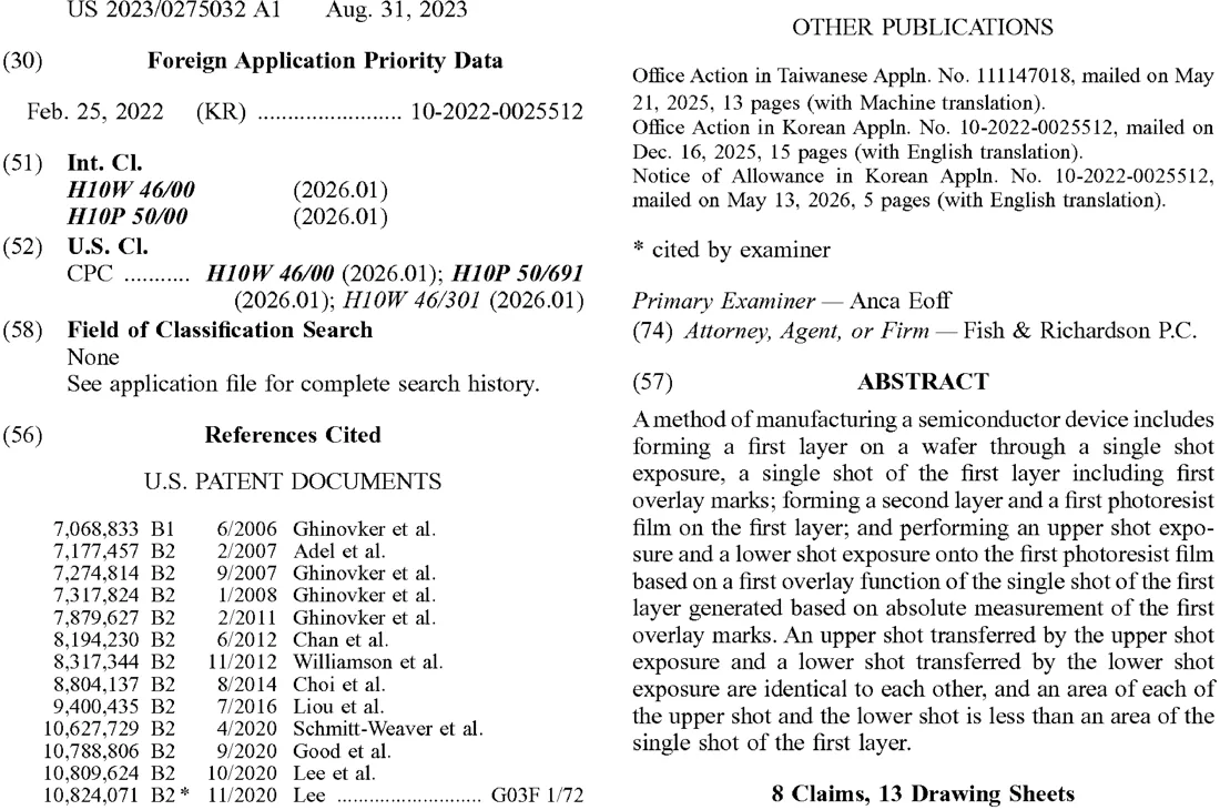
This patent describes a way to make computer chips by splitting a large image into two smaller parts. It uses reference marks on the first layer to ensure the top and bottom parts line up perfectly during manufacturing.
In the filing’s own words
A method of manufacturing a semiconductor device includes forming a first layer on a wafer through a single shot exposure, a single shot of the first layer including first overlay marks; forming a second layer and a first photoresist film on the first layer; and performing an upper shot exposure and a lower shot exposure onto the first photoresist film based on a first overlay function of the single shot of the first layer generated based on absolute measurement of the first overlay marks. An upper shot transferred by the upper shot exposure and a lower shot transferred by the lower shot exposure are identical to each other, and an area of each of the upper shot and the lower shot is less than an area of the single shot of the first layer.
What exactly they claim (claim 1)
1. A method of manufacturing a semiconductor device, the method comprising: forming a first layer on a wafer through a single shot exposure, a single shot of the first layer including first overlay marks; forming a second layer and a first photoresist film on the first layer; and performing an upper shot exposure and a lower shot exposure onto the first photoresist film based on a first overlay function of the single shot of the first layer generated based on absolute measurement of the first overlay marks, wherein an upper shot transferred by the upper shot exposure and a lower shot transferred by the lower shot exposure are identical to each other, and an area of each of the upper shot and the lower shot is less than an area of the single shot of the first layer.
Facts
- Company
- Samsung (Samsung Electronics Co., Ltd.)
- Official title
- Method of manufacturing semiconductor device
- Patent number
- US12757741B2
- Application number
- 18051639
- Filed
- Nov 1, 2022
- Granted
- Oct 6, 2026
- Inventors
- 2
- Claims
- 8
Classified under
H10W 46/00 Electricity & electronicsH10P 50/691 Electricity & electronicsH10W 46/301 Electricity & electronicsMore from Samsung in Chips & hardware
- Samsung patents chip that combines camera and screen Oct 13, 2026
- Samsung patents faster chip testing using machine learning Sep 1, 2026
- Samsung patents radar method to pinpoint target direction more accurately Sep 1, 2026
- Samsung patents memory chip that searches data by content, not address Sep 1, 2026
- Samsung patents chip design that skips empty data to speed up AI Sep 1, 2026
Summaries are simplified from the filing’s own abstract and first claim. A patent filing is not a product announcement.
Patent data and drawings: U.S. Patent and Trademark Office (USPTO). Nebula is not affiliated with or endorsed by the USPTO.